

AD7572AJN10
Product Overview
Category
AD7572AJN10 belongs to the category of analog-to-digital converters (ADCs).
Use
This product is primarily used for converting analog signals into digital data, making it suitable for various applications in industries such as telecommunications, industrial automation, and medical equipment.
Characteristics
- High precision: AD7572AJN10 offers a resolution of 10 bits, ensuring accurate conversion of analog signals.
- Fast conversion rate: With a maximum sampling rate of 1 megasample per second (MSPS), this ADC can handle high-speed signal processing requirements.
- Low power consumption: The AD7572AJN10 operates at low power levels, making it energy-efficient and suitable for battery-powered devices.
- Wide input voltage range: It supports a wide input voltage range, allowing for versatile signal acquisition.
Package
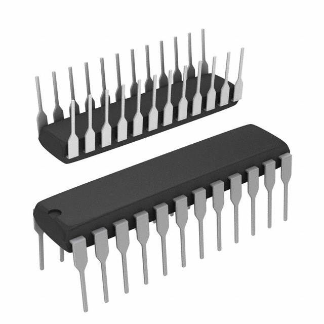
The AD7572AJN10 comes in a 28-pin plastic dual in-line package (DIP), which provides ease of integration into various electronic systems.
Essence
The essence of AD7572AJN10 lies in its ability to accurately convert analog signals into digital form, enabling further digital processing and analysis.
Packaging/Quantity
This product is typically packaged in reels or tubes, with each containing a specific quantity of AD7572AJN10 units. The exact packaging and quantity may vary depending on the supplier.
Specifications
- Resolution: 10 bits
- Sampling Rate: Up to 1 MSPS
- Input Voltage Range: ±10V
- Power Supply: +5V
- Operating Temperature Range: -40°C to +85°C
Detailed Pin Configuration
The AD7572AJN10 has a total of 28 pins, each serving a specific function. Here is a detailed pin configuration:
- VREF-
- VREF+
- AGND
- VIN-
- VIN+
- VDD
- D0
- D1
- D2
- D3
- D4
- D5
- D6
- D7
- D8
- D9
- WR
- RD
- CS
- SCLK
- DGND
- REFOUT
- CLKIN
- INT/CONVST
- BUSY
- RESET
- VLOGIC
- VREF
Functional Features
- High-resolution analog-to-digital conversion
- Fast sampling rate for real-time signal acquisition
- Low power consumption for energy-efficient operation
- Wide input voltage range for versatile signal handling
- Easy integration into electronic systems with standard package and pin configuration
Advantages and Disadvantages
Advantages
- Accurate and precise analog-to-digital conversion
- High-speed signal processing capabilities
- Energy-efficient operation
- Versatile input voltage range
Disadvantages
- Limited resolution compared to higher-bit ADCs
- Requires external components for complete functionality
Working Principles
The AD7572AJN10 operates based on the successive approximation register (SAR) architecture. It utilizes a capacitor array and a comparator to perform the analog-to-digital conversion process. The SAR algorithm compares the input analog voltage against a reference voltage and iteratively determines the digital representation of the input signal.
Detailed Application Field Plans
The AD7572AJN10 finds applications in various fields, including:
- Telecommunications: Used for signal processing in communication systems, such as base stations and modems.
- Industrial Automation: Enables precise measurement and control in industrial automation processes.
- Medical Equipment: Utilized in medical devices for accurate data acquisition and analysis.
- Test and Measurement: Suitable for test equipment, data loggers, and other measurement devices.
Detailed and Complete Alternative Models
- AD7572AJN12: Similar to AD7572AJN10 but with a resolution of 12 bits.
- AD7572AJN8: Similar to AD7572AJN10 but with a lower resolution of 8 bits.
- AD7572AJNZ: A surface-mount version of the AD7572AJN10 with similar specifications.
These alternative models provide options with varying resolutions and package types to suit different application requirements.
In conclusion, the AD7572AJN10 is a high-precision analog-to-digital converter that offers fast conversion rates and low power consumption. Its wide input voltage range and standard package make it suitable for various applications in telecommunications, industrial automation, medical equipment, and test and measurement fields. While it has limitations in terms of resolution and external component requirements, alternative models are available to cater to specific needs.
Lista 10 Vanliga frågor och svar relaterade till tillämpningen av AD7572AJN10 i tekniska lösningar
Sure! Here are 10 common questions and answers related to the application of AD7572AJN10 in technical solutions:
Q: What is the AD7572AJN10? A: The AD7572AJN10 is a 12-bit successive approximation analog-to-digital converter (ADC) manufactured by Analog Devices.
Q: What is the resolution of the AD7572AJN10? A: The AD7572AJN10 has a resolution of 12 bits, meaning it can represent analog signals with 2^12 (4096) discrete levels.
Q: What is the maximum sampling rate of the AD7572AJN10? A: The AD7572AJN10 has a maximum sampling rate of 100 kilosamples per second (ksps).
Q: What is the supply voltage range for the AD7572AJN10? A: The AD7572AJN10 operates from a single power supply voltage ranging from 4.5V to 5.5V.
Q: What is the input voltage range of the AD7572AJN10? A: The AD7572AJN10 has an input voltage range of 0V to Vref, where Vref is the reference voltage provided to the ADC.
Q: Does the AD7572AJN10 require an external reference voltage? A: Yes, the AD7572AJN10 requires an external reference voltage to determine the full-scale range of the ADC.
Q: What is the interface used to communicate with the AD7572AJN10? A: The AD7572AJN10 uses a parallel interface to communicate with microcontrollers or other digital devices.
Q: Can the AD7572AJN10 operate in a multi-channel configuration? A: Yes, the AD7572AJN10 can be used in multi-channel configurations by using multiple ADCs and multiplexing the inputs.
Q: What is the typical power consumption of the AD7572AJN10? A: The AD7572AJN10 has a typical power consumption of 5 milliwatts (mW) during normal operation.
Q: Are there any special considerations for PCB layout when using the AD7572AJN10? A: Yes, it is recommended to follow the guidelines provided in the datasheet for proper grounding, decoupling, and signal routing to minimize noise and ensure accurate performance.
Please note that these answers are general and may vary depending on specific application requirements. It is always recommended to refer to the datasheet and consult with Analog Devices or technical experts for detailed information and support.