

ADP5070ACPZ
Product Overview
- Category: Integrated Circuit (IC)
- Use: Power Management
- Characteristics: High Efficiency, Low Power Consumption
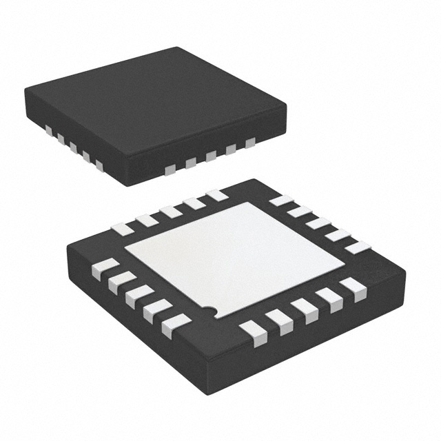
- Package: LFCSP (Lead Frame Chip Scale Package)
- Essence: Voltage Regulator
- Packaging/Quantity: Tape and Reel, 2500 units per reel
Specifications
- Input Voltage Range: 2.7V to 5.5V
- Output Voltage Range: 0.6V to 3.3V
- Maximum Output Current: 1A
- Quiescent Current: 30µA
- Switching Frequency: 2MHz
- Operating Temperature Range: -40°C to +85°C
Pin Configuration
The ADP5070ACPZ has the following pin configuration:
- VIN: Input Voltage
- SW1: Switch Node 1
- SW2: Switch Node 2
- GND: Ground
- FB1: Feedback Node 1
- FB2: Feedback Node 2
- EN: Enable Pin
- VOUT: Output Voltage
- PGND: Power Ground
Functional Features
- Dual Synchronous Buck Converters
- Adjustable Output Voltage
- Soft Start and Shutdown
- Overcurrent Protection
- Thermal Shutdown Protection
- Power Good Indicator
Advantages and Disadvantages
Advantages: - High Efficiency Conversion - Low Power Consumption - Small Package Size - Wide Input Voltage Range
Disadvantages: - Limited Maximum Output Current - Requires External Components for Operation
Working Principles
The ADP5070ACPZ is a dual synchronous buck converter that regulates the input voltage to a desired output voltage. It utilizes pulse-width modulation (PWM) techniques to control the switching of the internal power MOSFETs. The feedback nodes continuously monitor the output voltage and adjust the duty cycle of the switches to maintain a stable output.
Detailed Application Field Plans
The ADP5070ACPZ is commonly used in various applications, including but not limited to: - Portable Electronic Devices - Battery-Powered Systems - Industrial Control Systems - Automotive Electronics - Telecommunications Equipment
Alternative Models
Some alternative models that can be considered as alternatives to the ADP5070ACPZ are: - LM2576-ADJ - LT1763-3.3 - TPS5430-3.3 - MAX5033AUPA - MCP1702-3302E
These models offer similar functionality and can be suitable replacements depending on specific requirements.
In conclusion, the ADP5070ACPZ is a versatile power management IC that provides efficient voltage regulation for various electronic devices. Its compact size, wide input voltage range, and adjustable output voltage make it suitable for a wide range of applications. However, its limited maximum output current and requirement for external components should be taken into consideration during design.
Lista 10 Vanliga frågor och svar relaterade till tillämpningen av ADP5070ACPZ i tekniska lösningar
Sure! Here are 10 common questions and answers related to the application of ADP5070ACPZ in technical solutions:
Q: What is ADP5070ACPZ? A: ADP5070ACPZ is a high-performance, dual-channel power management IC designed for use in various technical solutions.
Q: What are the key features of ADP5070ACPZ? A: ADP5070ACPZ features include dual buck converters, integrated LDOs, programmable power sequencing, fault protection, and a wide input voltage range.
Q: What is the input voltage range supported by ADP5070ACPZ? A: ADP5070ACPZ supports an input voltage range from 4.5V to 20V.
Q: How many buck converters are there in ADP5070ACPZ? A: ADP5070ACPZ has two integrated buck converters, each capable of delivering up to 2A of output current.
Q: Can I program the power sequencing of ADP5070ACPZ? A: Yes, ADP5070ACPZ allows you to program the power sequencing through its I2C interface, enabling flexible control over the power-up and power-down sequence.
Q: Does ADP5070ACPZ provide any fault protection features? A: Yes, ADP5070ACPZ offers various fault protection features such as overvoltage protection (OVP), undervoltage lockout (UVLO), and thermal shutdown.
Q: What are the applications of ADP5070ACPZ? A: ADP5070ACPZ can be used in a wide range of applications, including industrial automation, telecommunications, data centers, and automotive systems.
Q: Can ADP5070ACPZ operate in a wide temperature range? A: Yes, ADP5070ACPZ is designed to operate reliably in a temperature range from -40°C to +125°C.
Q: Does ADP5070ACPZ require any external components for operation? A: Yes, ADP5070ACPZ requires external input and output capacitors, as well as inductors for each buck converter.
Q: Is there any evaluation board available for ADP5070ACPZ? A: Yes, Analog Devices provides an evaluation board for ADP5070ACPZ, which can help in the development and testing of your technical solution.
Please note that these answers are general and may vary depending on specific requirements and use cases. It's always recommended to refer to the datasheet and consult with the manufacturer for detailed information.