

CY62256L-70PC
Product Overview
Category
CY62256L-70PC belongs to the category of static random access memory (SRAM) chips.
Use
This product is primarily used as a high-speed, low-power memory solution in various electronic devices and systems.
Characteristics
- High speed: The CY62256L-70PC offers fast access times, making it suitable for applications that require quick data retrieval.
- Low power consumption: This SRAM chip is designed to operate efficiently with minimal power consumption.
- Reliable performance: The CY62256L-70PC provides reliable data storage and retrieval capabilities.
- Compact package: It comes in a compact package, allowing for easy integration into different electronic devices.
- Large storage capacity: This chip has a storage capacity of 32 kilobits (32K), providing ample space for data storage.
Package and Quantity
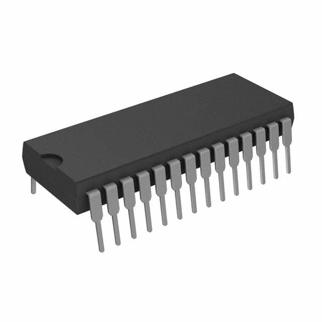
The CY62256L-70PC is available in a standard 28-pin plastic dual in-line package (PDIP). It is typically sold in quantities of one or more units per package.
Specifications
- Access Time: 70 nanoseconds (ns)
- Operating Voltage: 5 volts (V)
- Standby Current: 10 microamps (μA)
- Operating Temperature Range: -40°C to +85°C
- Data Retention: More than 20 years
Pin Configuration
The CY62256L-70PC follows the industry-standard pin configuration for 28-pin PDIP packages. The detailed pinout is as follows:
- Chip Enable (CE)
- Output Enable (OE)
- Write Enable (WE)
- Address Inputs (A0-A13)
- Data Inputs/Outputs (DQ0-DQ7)
- Power Supply (+5V)
- Ground (GND)
Note: The remaining pins are not listed here for brevity.
Functional Features
- Chip Enable (CE): Activates the chip and enables data access.
- Output Enable (OE): Controls the output buffer, allowing data to be read from the chip.
- Write Enable (WE): Enables write operations to the memory.
- Address Inputs (A0-A13): Selects the memory location to read from or write to.
- Data Inputs/Outputs (DQ0-DQ7): Bi-directional pins for data transfer between the chip and external devices.
- Power Supply (+5V): Provides the necessary power for the chip's operation.
- Ground (GND): Serves as the reference voltage for the chip.
Advantages and Disadvantages
Advantages
- High-speed performance allows for quick data access.
- Low power consumption helps conserve energy in electronic systems.
- Reliable data storage and retrieval capabilities ensure data integrity.
- Compact package facilitates easy integration into various devices.
- Ample storage capacity for many applications.
Disadvantages
- Limited storage capacity compared to other memory technologies.
- Requires a 5V power supply, which may not be compatible with all systems.
- Relatively higher cost compared to some alternative memory solutions.
Working Principles
The CY62256L-70PC operates based on the principles of static random access memory. It stores data using flip-flops, which retain their state until power is removed. The chip uses address inputs to select specific memory locations and allows data to be read from or written to those locations. The control signals (CE, OE, WE) determine the type of operation (read or write) and enable the appropriate circuitry within the chip.
Application Field Plans
The CY62256L-70PC finds application in various electronic systems, including but not limited to: - Microcontrollers - Embedded systems - Communication devices - Industrial automation - Medical equipment
Alternative Models
Several alternative models with similar specifications and functionalities to the CY62256L-70PC are available in the market. Some notable alternatives include: - CY62256N-70PC - KM62256CLP-7 - M5M5256BFP-70LL
These alternative models can be considered based on specific requirements and availability.
In conclusion, the CY62256L-70PC is a high-speed, low-power SRAM chip that offers reliable data storage and retrieval capabilities. With its compact package and ample storage capacity, it finds applications in various electronic systems. While it has certain limitations, such as limited storage capacity and higher cost compared to some alternatives, it remains a popular choice for many applications requiring fast and efficient memory solutions.
Lista 10 Vanliga frågor och svar relaterade till tillämpningen av CY62256L-70PC i tekniska lösningar
Sure! Here are 10 common questions and answers related to the application of CY62256L-70PC in technical solutions:
Q: What is CY62256L-70PC? A: CY62256L-70PC is a 32K x 8 Static Random Access Memory (SRAM) chip manufactured by Cypress Semiconductor.
Q: What is the operating voltage range for CY62256L-70PC? A: The operating voltage range for CY62256L-70PC is typically between 4.5V and 5.5V.
Q: What is the maximum clock frequency supported by CY62256L-70PC? A: CY62256L-70PC can support a maximum clock frequency of 70 MHz.
Q: What is the access time of CY62256L-70PC? A: The access time of CY62256L-70PC is 70 ns.
Q: Can CY62256L-70PC be used in battery-powered devices? A: Yes, CY62256L-70PC can be used in battery-powered devices as it operates within a typical voltage range suitable for such applications.
Q: Is CY62256L-70PC compatible with both 3.3V and 5V logic levels? A: No, CY62256L-70PC is designed to work with 5V logic levels. For 3.3V compatibility, you may need level-shifting circuitry.
Q: How much data can CY62256L-70PC store? A: CY62256L-70PC has a storage capacity of 32 kilobits or 4 kilobytes.
Q: Can CY62256L-70PC be used as a cache memory in microcontrollers? A: Yes, CY62256L-70PC can be used as a cache memory in microcontrollers to improve data access speed.
Q: Does CY62256L-70PC support simultaneous read and write operations? A: No, CY62256L-70PC does not support simultaneous read and write operations. It is a synchronous memory device.
Q: What are some typical applications of CY62256L-70PC? A: CY62256L-70PC is commonly used in various technical solutions such as embedded systems, industrial control systems, telecommunications equipment, and automotive electronics.
Please note that the answers provided here are general and may vary depending on specific design requirements and application scenarios.