

CY7C0852V-133BBI
Product Overview
Category
The CY7C0852V-133BBI belongs to the category of integrated circuits (ICs).
Use
This IC is commonly used in electronic devices for various applications, including data storage, communication systems, and digital signal processing.
Characteristics
- High-speed performance: The CY7C0852V-133BBI operates at a high clock frequency, enabling fast data processing.
- Large storage capacity: This IC offers a significant amount of memory, allowing for the storage of large amounts of data.
- Low power consumption: It is designed to minimize power usage, making it suitable for battery-powered devices.
- Reliable operation: The CY7C0852V-133BBI is known for its stability and durability, ensuring consistent performance over time.
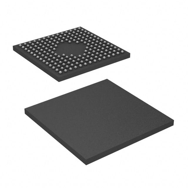
Package
The CY7C0852V-133BBI is available in a compact and standardized package, which facilitates easy integration into electronic circuit boards.
Essence
The essence of the CY7C0852V-133BBI lies in its ability to provide high-speed data storage and processing capabilities, making it an essential component in modern electronic devices.
Packaging/Quantity
This IC is typically sold in reels or trays, with each reel or tray containing a specific quantity of units. The exact packaging and quantity may vary depending on the supplier.
Specifications
- Clock Frequency: 133 MHz
- Memory Capacity: 8 Megabits (1 Megabyte)
- Supply Voltage: 3.3V
- Operating Temperature Range: -40°C to +85°C
- Interface: Parallel
Detailed Pin Configuration
The CY7C0852V-133BBI features a standard pin configuration, as follows:
- VCC
- A0
- A1
- A2
- A3
- A4
- A5
- A6
- A7
- A8
- A9
- A10
- A11
- A12
- A13
- A14
- A15
- A16
- A17
- A18
- A19
- A20
- A21
- A22
- A23
- A24
- A25
- A26
- A27
- A28
- A29
- A30
- A31
- DQ0
- DQ1
- DQ2
- DQ3
- DQ4
- DQ5
- DQ6
- DQ7
- WE#
- OE#
- CE#
- BYTE#
- UB#
- LB#
- VSS
Functional Features
The CY7C0852V-133BBI offers the following functional features:
- Random Access Memory (RAM): It allows for fast read and write operations, enabling efficient data storage and retrieval.
- Address Decoding: The IC supports address decoding, which facilitates easy access to specific memory locations.
- Data Bus Interface: It provides a parallel interface for seamless communication with other components in the system.
- Control Signals: The CY7C0852V-133BBI includes various control signals such as Write Enable (WE#), Output Enable (OE#), and Chip Enable (CE#), allowing for precise control over data operations.
Advantages and Disadvantages
Advantages
- High-speed performance enables quick data processing.
- Large storage capacity accommodates significant amounts of data.
- Low power consumption prolongs battery life in portable devices.
- Reliable operation ensures consistent performance over time.
Disadvantages
- Limited memory capacity compared to newer ICs with higher storage capabilities.
- Parallel interface may not be suitable for certain applications requiring serial communication.
Working Principles
The CY7C0852V-133BBI operates based on the principles of random access memory. It stores data in a matrix of memory cells, each identified by a unique address. The IC utilizes control signals to read from or write to specific memory locations. When a read operation is initiated, the requested data is retrieved and made available on the data bus. Similarly, during a write operation, data is written to the specified memory location.
Detailed Application Field Plans
The CY7C0852V-133BBI finds application in various fields, including:
- Computer Systems: Used as cache memory or main memory in computer systems to enhance data processing speed.
- Communication Systems: Employed in networking equipment and routers for buffering and storing data packets.
- Consumer Electronics: Integrated into devices such as digital cameras, printers, and set-top boxes
Lista 10 Vanliga frågor och svar relaterade till tillämpningen av CY7C0852V-133BBI i tekniska lösningar
Sure! Here are 10 common questions and answers related to the application of CY7C0852V-133BBI in technical solutions:
Question: What is the CY7C0852V-133BBI?
Answer: The CY7C0852V-133BBI is a specific model of synchronous SRAM (Static Random Access Memory) chip.Question: What is the capacity of the CY7C0852V-133BBI?
Answer: The CY7C0852V-133BBI has a capacity of 8 megabits (Mb).Question: What is the operating voltage range for the CY7C0852V-133BBI?
Answer: The operating voltage range for this chip is typically between 3.0V and 3.6V.Question: What is the maximum clock frequency supported by the CY7C0852V-133BBI?
Answer: The CY7C0852V-133BBI can support a maximum clock frequency of 133 MHz.Question: What is the access time of the CY7C0852V-133BBI?
Answer: The access time for this chip is typically 8 ns.Question: Can the CY7C0852V-133BBI be used in industrial applications?
Answer: Yes, the CY7C0852V-133BBI is suitable for use in industrial applications due to its robust design and reliability.Question: Does the CY7C0852V-133BBI have any built-in error correction capabilities?
Answer: No, the CY7C0852V-133BBI does not have built-in error correction capabilities. Additional error correction mechanisms may need to be implemented if required.Question: What is the package type of the CY7C0852V-133BBI?
Answer: The CY7C0852V-133BBI comes in a 44-pin TSOP (Thin Small Outline Package) form factor.Question: Can the CY7C0852V-133BBI be used in automotive applications?
Answer: Yes, the CY7C0852V-133BBI is suitable for use in automotive applications as it can withstand extended temperature ranges and has high reliability.Question: Are there any specific design considerations when using the CY7C0852V-133BBI?
Answer: It is important to ensure proper decoupling capacitors are used near the power supply pins of the chip to minimize noise and voltage fluctuations. Additionally, attention should be given to signal integrity and timing requirements in the overall system design.
Please note that these answers are general and may vary depending on the specific requirements and application of the CY7C0852V-133BBI in a technical solution.