

CY7C1049B-17VC
Product Overview
Category
The CY7C1049B-17VC belongs to the category of integrated circuits (ICs).
Use
This IC is commonly used in electronic devices for data storage and retrieval purposes.
Characteristics
- High-speed performance
- Low power consumption
- Reliable operation
- Compact size
Package
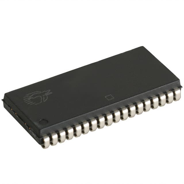
The CY7C1049B-17VC is available in a small outline integrated circuit (SOIC) package.
Essence
The essence of this product lies in its ability to efficiently store and retrieve data in electronic devices.
Packaging/Quantity
The CY7C1049B-17VC is typically packaged in reels or tubes, with a quantity of 250 units per reel/tube.
Specifications
- Operating Voltage: 3.3V
- Access Time: 17ns
- Memory Size: 1 Megabit (128K x 8)
- Organization: 128K words x 8 bits
- Interface: Parallel
- Operating Temperature Range: -40°C to +85°C
Detailed Pin Configuration
The CY7C1049B-17VC has a total of 28 pins. The pin configuration is as follows:
- A0
- A1
- A2
- A3
- A4
- A5
- A6
- A7
- VCC
- CE#
- OE#
- WE#
- I/O0
- I/O1
- I/O2
- I/O3
- I/O4
- I/O5
- I/O6
- I/O7
- GND
- NC
- NC
- NC
- NC
- NC
- NC
- NC
Functional Features
- High-speed data access
- Low power consumption in standby mode
- Easy integration into existing electronic systems
- Reliable operation under various environmental conditions
Advantages and Disadvantages
Advantages
- Fast data access time
- Low power consumption
- Compact size for space-constrained applications
- Wide operating temperature range
Disadvantages
- Limited memory size (1 Megabit)
- Parallel interface may not be suitable for all applications
- Higher cost compared to lower-capacity memory options
Working Principles
The CY7C1049B-17VC operates based on the principles of static random-access memory (SRAM). It stores data in a volatile manner, meaning that the stored information is lost when power is removed. The IC utilizes an address bus to select specific memory locations and a data bus to read from or write to those locations.
Detailed Application Field Plans
The CY7C1049B-17VC finds application in various electronic devices, including but not limited to: - Computer motherboards - Networking equipment - Industrial control systems - Automotive electronics - Consumer electronics
Detailed and Complete Alternative Models
- CY7C1049BV33-15ZI - 1 Megabit SRAM, 3.3V, 15ns access time, TSOP package
- CY7C1049CV33-10ZXC - 1 Megabit SRAM, 3.3V, 10ns access time, BGA package
- CY7C1049DV33-12SXI - 1 Megabit SRAM, 3.3V, 12ns access time, SOJ package
- CY7C1049EV33-20AXC - 1 Megabit SRAM, 3.3V, 20ns access time, TQFP package
These alternative models offer similar functionality and performance but may differ in package type, access time, or other specifications.
In conclusion, the CY7C1049B-17VC is a high-speed, low-power SRAM IC that provides reliable data storage and retrieval capabilities. Its compact size and wide operating temperature range make it suitable for various electronic applications. However, its limited memory size and parallel interface may pose limitations in certain scenarios.
Lista 10 Vanliga frågor och svar relaterade till tillämpningen av CY7C1049B-17VC i tekniska lösningar
Sure! Here are 10 common questions and answers related to the application of CY7C1049B-17VC in technical solutions:
Question: What is the maximum operating frequency of CY7C1049B-17VC?
Answer: The maximum operating frequency of CY7C1049B-17VC is 166 MHz.Question: What is the voltage supply range for CY7C1049B-17VC?
Answer: CY7C1049B-17VC operates with a voltage supply range of 3.0V to 3.6V.Question: Can CY7C1049B-17VC be used in low-power applications?
Answer: Yes, CY7C1049B-17VC has a low-power standby mode that can be utilized for power-saving purposes.Question: What is the capacity of CY7C1049B-17VC?
Answer: CY7C1049B-17VC is a 4 Meg x 9 synchronous FIFO memory with a total capacity of 36 Megabits.Question: Does CY7C1049B-17VC support multiple clock domains?
Answer: Yes, CY7C1049B-17VC supports independent read and write clocks, making it suitable for systems with multiple clock domains.Question: Can CY7C1049B-17VC be cascaded with other FIFO devices?
Answer: Yes, CY7C1049B-17VC can be easily cascaded with other FIFO devices to increase the overall memory depth.Question: What is the access time of CY7C1049B-17VC?
Answer: The access time of CY7C1049B-17VC is 17 ns, hence the "17VC" in its part number.Question: Does CY7C1049B-17VC have any built-in error detection or correction mechanisms?
Answer: No, CY7C1049B-17VC does not have built-in error detection or correction mechanisms. It is a basic synchronous FIFO memory.Question: Can CY7C1049B-17VC be used in high-speed data acquisition systems?
Answer: Yes, CY7C1049B-17VC can be used in high-speed data acquisition systems due to its fast access time and high operating frequency.Question: Is CY7C1049B-17VC compatible with different interface standards?
Answer: Yes, CY7C1049B-17VC supports various interface standards such as LVTTL, LVCMOS, and LVPECL, making it versatile for different applications.
Please note that these answers are based on general information about CY7C1049B-17VC and may vary depending on specific implementation requirements.