

CY7C1049GE30-10ZSXI
Product Overview
Category
The CY7C1049GE30-10ZSXI belongs to the category of synchronous static random access memory (SRAM) chips.
Use
This product is primarily used in electronic devices and systems that require high-speed and reliable data storage and retrieval.
Characteristics
- Synchronous operation: The CY7C1049GE30-10ZSXI operates synchronously with the system clock, allowing for efficient data transfer.
- High-speed performance: With a maximum operating frequency of 100 MHz, this SRAM chip offers fast read and write operations.
- Low power consumption: The CY7C1049GE30-10ZSXI is designed to minimize power consumption, making it suitable for battery-powered devices.
- High density: This chip has a capacity of 1 Megabit (128K x 8), providing ample storage space for data.
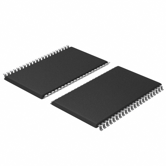
Package
The CY7C1049GE30-10ZSXI is available in a small outline integrated circuit (SOIC) package. This package ensures easy integration into various electronic systems.
Essence
The essence of the CY7C1049GE30-10ZSXI lies in its ability to provide high-speed and reliable data storage in a compact form factor.
Packaging/Quantity
This SRAM chip is typically packaged in reels or trays, with each reel containing a specific quantity of chips. The exact packaging and quantity may vary depending on the supplier.
Specifications
- Organization: 128K x 8 bits
- Operating Voltage: 3.3V
- Access Time: 10 ns
- Operating Temperature Range: -40°C to +85°C
- Data Retention: Greater than 20 years
Detailed Pin Configuration
The CY7C1049GE30-10ZSXI has a total of 32 pins, which are assigned specific functions. The pin configuration is as follows:
- Chip Enable (CE)
- Output Enable (OE)
- Write Enable (WE)
- Address Inputs (A0-A16)
- Data Inputs/Outputs (DQ0-DQ7)
- Power Supply (VCC)
- Ground (GND)
Please refer to the datasheet for a complete pin diagram and detailed pin descriptions.
Functional Features
- Asynchronous and synchronous operation modes: The CY7C1049GE30-10ZSXI can be operated in both asynchronous and synchronous modes, providing flexibility in different system configurations.
- Burst mode support: This SRAM chip supports burst read and write operations, allowing for efficient data transfer in burst-oriented applications.
- Automatic power-down: The CY7C1049GE30-10ZSXI features an automatic power-down mode, reducing power consumption when the chip is not actively accessed.
- Built-in error detection and correction: This chip incorporates error detection and correction circuitry, ensuring data integrity during storage and retrieval.
Advantages and Disadvantages
Advantages
- High-speed performance enables fast data access.
- Low power consumption makes it suitable for battery-powered devices.
- Compact form factor allows for easy integration into various electronic systems.
- Error detection and correction feature ensures data integrity.
Disadvantages
- Limited storage capacity compared to higher-density memory chips.
- Relatively higher cost per unit compared to other types of memory.
Working Principles
The CY7C1049GE30-10ZSXI operates by storing data in a matrix of memory cells. These cells consist of flip-flops that can store a single bit of information. The address inputs are used to select a specific memory location, while the data inputs/outputs facilitate the reading and writing of data.
During operation, the chip synchronizes its internal operations with the system clock. This synchronous operation ensures that data is transferred accurately and efficiently between the SRAM chip and the rest of the system.
Detailed Application Field Plans
The CY7C1049GE30-10ZSXI finds applications in various electronic devices and systems, including but not limited to:
- Computer systems: Used as cache memory or main memory in desktops, laptops, and servers.
- Networking equipment: Employed for packet buffering and data storage in routers, switches, and network appliances.
- Communication systems: Utilized for buffering and temporary storage in telecommunication devices and base stations.
- Industrial automation: Integrated into control systems and programmable logic controllers (PLCs) for data storage and retrieval.
- Automotive electronics: Used in automotive control units and infotainment systems for fast and reliable data storage.
Detailed and Complete Alternative Models
- CY7C1049G30-10ZSXE: Similar to the CY7C1049GE30-10ZSXI, this model offers the same specifications and features but comes in a
Lista 10 Vanliga frågor och svar relaterade till tillämpningen av CY7C1049GE30-10ZSXI i tekniska lösningar
Sure! Here are 10 common questions and answers related to the application of CY7C1049GE30-10ZSXI in technical solutions:
Question: What is the maximum operating frequency of CY7C1049GE30-10ZSXI?
Answer: The maximum operating frequency of CY7C1049GE30-10ZSXI is 100 MHz.Question: What is the voltage supply range for this device?
Answer: The voltage supply range for CY7C1049GE30-10ZSXI is 3.0V to 3.6V.Question: Can I use this device in a low-power application?
Answer: Yes, CY7C1049GE30-10ZSXI has a low-power standby mode that can be used to conserve power when not in use.Question: What is the maximum capacity of CY7C1049GE30-10ZSXI?
Answer: CY7C1049GE30-10ZSXI has a maximum capacity of 1 Megabit (128K x 8).Question: Does this device support multiple read and write operations simultaneously?
Answer: No, CY7C1049GE30-10ZSXI does not support simultaneous multiple read and write operations.Question: Can I use this device in industrial temperature environments?
Answer: Yes, CY7C1049GE30-10ZSXI is designed to operate in industrial temperature ranges (-40°C to +85°C).Question: Does this device have any built-in error correction mechanisms?
Answer: No, CY7C1049GE30-10ZSXI does not have built-in error correction mechanisms.Question: Can I cascade multiple CY7C1049GE30-10ZSXI devices together?
Answer: Yes, you can cascade multiple CY7C1049GE30-10ZSXI devices to increase the overall memory capacity.Question: What is the access time of this device?
Answer: The access time of CY7C1049GE30-10ZSXI is 10 ns.Question: Can I use this device in battery-powered applications?
Answer: Yes, CY7C1049GE30-10ZSXI has a low-power standby mode and can be used in battery-powered applications.
Please note that these answers are based on general information about the CY7C1049GE30-10ZSXI device. For specific technical details and application requirements, it is recommended to refer to the datasheet or consult with the manufacturer.