

S29JL064J70TFI003
Product Overview
- Category: Memory device
- Use: Data storage and retrieval
- Characteristics: High capacity, fast access speed, non-volatile, low power consumption
- Package: Integrated circuit (IC)
- Essence: Flash memory
- Packaging/Quantity: Individual ICs in anti-static packaging
Specifications
- Capacity: 64 megabits (8 megabytes)
- Access Speed: 70 nanoseconds
- Interface: Parallel
- Operating Voltage: 2.7V - 3.6V
- Operating Temperature: -40°C to +85°C
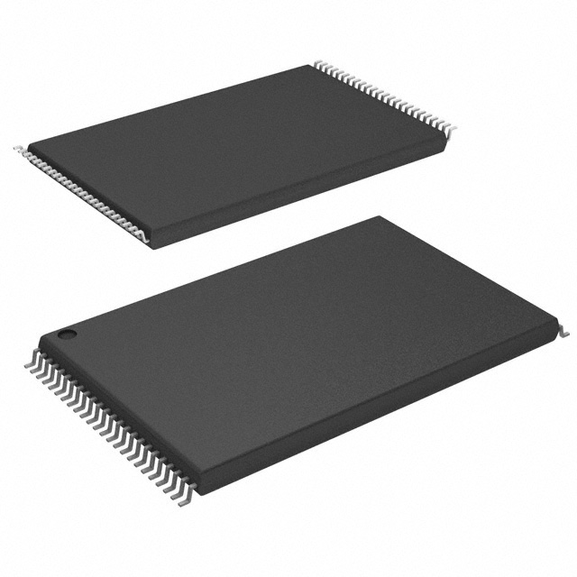
Detailed Pin Configuration
The S29JL064J70TFI003 has a total of 48 pins. The pin configuration is as follows:
- VCC: Power supply voltage
- A0-A18: Address inputs
- DQ0-DQ15: Data inputs/outputs
- WE#: Write enable
- CE#: Chip enable
- OE#: Output enable
- RP#/BYTE#: Reset/byte select
- RY/BY#: Ready/busy status
- WP#/ACC: Write protect/acceleration
- VSS: Ground
(Note: This is a simplified representation. Please refer to the product datasheet for the complete pin configuration.)
Functional Features
- High-speed data transfer
- Non-volatile storage
- Low power consumption
- Reliable and durable
- Easy integration into existing systems
- Support for various memory management techniques
Advantages and Disadvantages
Advantages: - Large storage capacity - Fast access speed - Low power consumption - Non-volatile (retains data even when power is off) - Versatile application possibilities
Disadvantages: - Relatively higher cost compared to other memory technologies - Limited endurance (limited number of erase/write cycles)
Working Principles
The S29JL064J70TFI003 is based on flash memory technology. It utilizes floating-gate transistors to store and retrieve data. When data is written, an electrical charge is trapped in the floating gate, altering the transistor's behavior. This charge can be removed during an erase operation, allowing the transistor to return to its original state. The stored data can be accessed by sending appropriate address signals and reading the corresponding data from the memory cells.
Detailed Application Field Plans
The S29JL064J70TFI003 is widely used in various applications that require non-volatile storage and fast access speed. Some common application fields include:
- Consumer Electronics: Used in digital cameras, portable media players, and gaming consoles for storing firmware, operating systems, and user data.
- Automotive: Integrated into automotive systems for storing critical data such as engine parameters, navigation maps, and entertainment content.
- Industrial Automation: Utilized in industrial control systems for storing program code, configuration data, and logged information.
- Networking Equipment: Incorporated into routers, switches, and network storage devices for caching, buffering, and storing network traffic data.
- Medical Devices: Employed in medical equipment for storing patient records, diagnostic data, and firmware updates.
Detailed and Complete Alternative Models
- S29GL064N90TFI010: Similar flash memory device with a larger capacity and faster access speed.
- AT25SF641: Serial flash memory with comparable capacity and access speed but different interface and package.
- MX25L6433F: Another alternative with similar specifications and functionality.
(Note: These are just a few examples. There are several alternative models available in the market.)
This entry provides an overview of the S29JL064J70TFI003 flash memory device. It includes information about its category, use, characteristics, package, specifications, pin configuration, functional features, advantages and disadvantages, working principles, application field plans, and alternative models.
Lista 10 Vanliga frågor och svar relaterade till tillämpningen av S29JL064J70TFI003 i tekniska lösningar
Sure! Here are 10 common questions and answers related to the application of S29JL064J70TFI003 in technical solutions:
Question: What is the S29JL064J70TFI003?
Answer: The S29JL064J70TFI003 is a specific model of flash memory chip manufactured by Cypress Semiconductor.Question: What is the capacity of the S29JL064J70TFI003?
Answer: The S29JL064J70TFI003 has a capacity of 64 megabits (8 megabytes).Question: What is the operating voltage range for this flash memory chip?
Answer: The S29JL064J70TFI003 operates within a voltage range of 2.7V to 3.6V.Question: What is the interface used to communicate with the S29JL064J70TFI003?
Answer: The S29JL064J70TFI003 uses a standard parallel interface for communication.Question: Can the S29JL064J70TFI003 be used in industrial applications?
Answer: Yes, the S29JL064J70TFI003 is designed to meet the requirements of industrial applications.Question: Does the S29JL064J70TFI003 support hardware data protection features?
Answer: Yes, the S29JL064J70TFI003 supports various hardware data protection features like block lock, password protection, and more.Question: What is the typical access time of the S29JL064J70TFI003?
Answer: The typical access time of the S29JL064J70TFI003 is around 70 nanoseconds.Question: Can the S29JL064J70TFI003 be used in automotive applications?
Answer: Yes, the S29JL064J70TFI003 is qualified for automotive applications and meets the necessary standards.Question: Does the S29JL064J70TFI003 support software write protection?
Answer: Yes, the S29JL064J70TFI003 supports software write protection through specific commands.Question: What is the temperature range within which the S29JL064J70TFI003 can operate?
Answer: The S29JL064J70TFI003 has an extended temperature range of -40°C to +85°C, making it suitable for various environments.
Please note that these answers are based on general information about the S29JL064J70TFI003 flash memory chip. For specific technical details and application requirements, it is recommended to refer to the official documentation provided by Cypress Semiconductor.