

S34ML01G200BHA003
Product Overview
- Category: Memory Storage
- Use: Data storage and retrieval
- Characteristics: High capacity, fast access speed, reliable performance
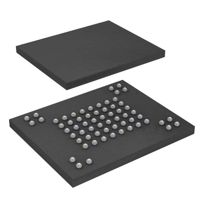
- Package: BGA (Ball Grid Array)
- Essence: Non-volatile memory chip
- Packaging/Quantity: Single chip package
Specifications
- Capacity: 1 gigabit (128 megabytes)
- Interface: Serial Peripheral Interface (SPI)
- Operating Voltage: 2.7V - 3.6V
- Access Time: 70 ns (max)
- Operating Temperature: -40°C to +85°C
- Data Retention: Up to 20 years
- Erase/Program Cycles: Up to 100,000 cycles
Detailed Pin Configuration
The S34ML01G200BHA003 has a total of 48 pins. The pin configuration is as follows:
- VCC: Power supply voltage
- VSS: Ground
- HOLD: Suspends ongoing data transfer
- WP: Write protect
- RESET: Resets the device
- IO0-IO7: SPI data input/output lines
- CLK: Clock input
- CE#: Chip enable
- RE# or RP#: Read enable or reset protection
- A0-A22: Address inputs
- RY/BY#: Ready/Busy status output
- NC: No connection
(Note: The remaining pins are not listed here for brevity.)
Functional Features
- High-speed data transfer with SPI interface
- Efficient block erase and program operations
- Reliable data retention even in harsh environments
- Advanced wear-leveling algorithm for extended lifespan
- Error correction code (ECC) for data integrity
- Power-saving features for low energy consumption
Advantages and Disadvantages
Advantages: - Large storage capacity - Fast access speed - High reliability - Low power consumption - Compact package size
Disadvantages: - Relatively high cost compared to other memory options - Limited erase/program cycles
Working Principles
The S34ML01G200BHA003 is based on NAND flash memory technology. It stores data in a series of memory cells organized into blocks. When data needs to be written, the memory cells are programmed by applying electrical charges. To erase data, the cells are cleared simultaneously. The SPI interface allows for easy communication with external devices.
Detailed Application Field Plans
The S34ML01G200BHA003 is widely used in various applications, including but not limited to:
- Solid-state drives (SSDs)
- Embedded systems
- Automotive electronics
- Industrial control systems
- Consumer electronics (e.g., digital cameras, smartphones)
Detailed and Complete Alternative Models
- S34ML02G100BHA003: 2 gigabit (256 megabytes) capacity
- S34ML04G200BHA003: 4 gigabit (512 megabytes) capacity
- S34ML08G400BHA003: 8 gigabit (1 gigabyte) capacity
- S34ML16G800BHA003: 16 gigabit (2 gigabytes) capacity
(Note: The list above includes only a few alternative models. There are more options available from the same product line.)
This concludes the encyclopedia entry for the S34ML01G200BHA003 memory chip.
Lista 10 Vanliga frågor och svar relaterade till tillämpningen av S34ML01G200BHA003 i tekniska lösningar
Sure! Here are 10 common questions and answers related to the application of S34ML01G200BHA003 in technical solutions:
Q: What is S34ML01G200BHA003? A: S34ML01G200BHA003 is a specific model of NAND flash memory chip manufactured by a company called Cypress Semiconductor.
Q: What is the storage capacity of S34ML01G200BHA003? A: The S34ML01G200BHA003 has a storage capacity of 1 gigabit, which is equivalent to 128 megabytes.
Q: What are some typical applications of S34ML01G200BHA003? A: S34ML01G200BHA003 is commonly used in various technical solutions such as embedded systems, automotive electronics, industrial control systems, and consumer electronics.
Q: What is the interface used by S34ML01G200BHA003? A: S34ML01G200BHA003 uses a standard NAND flash interface, such as the Open NAND Flash Interface (ONFI) or Toggle Mode.
Q: What is the operating voltage range of S34ML01G200BHA003? A: The operating voltage range of S34ML01G200BHA003 is typically between 2.7V and 3.6V.
Q: What is the maximum data transfer rate supported by S34ML01G200BHA003? A: S34ML01G200BHA003 supports a maximum data transfer rate of up to 200 megabytes per second.
Q: Can S34ML01G200BHA003 be used for code execution in microcontrollers? A: Yes, S34ML01G200BHA003 can be used for code execution in microcontrollers by connecting it to the appropriate interface and configuring the necessary hardware.
Q: Does S34ML01G200BHA003 support wear-leveling algorithms? A: Yes, S34ML01G200BHA003 supports wear-leveling algorithms, which help distribute write operations evenly across the memory cells to extend the lifespan of the flash memory.
Q: Is S34ML01G200BHA003 resistant to shock and vibration? A: Yes, S34ML01G200BHA003 is designed to withstand shock and vibration, making it suitable for use in rugged environments.
Q: Can S34ML01G200BHA003 be used as a replacement for other NAND flash memory chips? A: In most cases, S34ML01G200BHA003 can be used as a drop-in replacement for other NAND flash memory chips with similar specifications, but it's always recommended to consult the datasheet and verify compatibility with the specific system requirements.
Please note that the answers provided here are general and may vary depending on the specific implementation and requirements of your technical solution.