

S34ML01G200BHI500
Product Overview
- Category: NAND Flash Memory
- Use: Data storage in electronic devices
- Characteristics: High capacity, fast data transfer rate, reliable performance
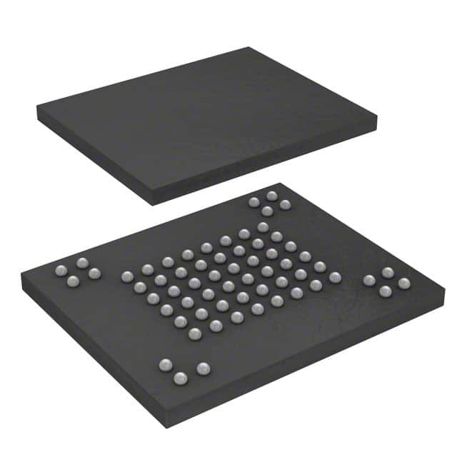
- Package: BGA (Ball Grid Array)
- Essence: Non-volatile memory for long-term data storage
- Packaging/Quantity: Available in reels, quantity varies based on customer requirements
Specifications
- Capacity: 1 Gb (Gigabit)
- Interface: Toggle Mode 2.0
- Voltage: 2.7V - 3.6V
- Operating Temperature: -40°C to +85°C
- Data Transfer Rate: Up to 400 Mbps (Megabits per second)
- Endurance: Up to 100,000 program/erase cycles
- Retention: Up to 10 years
Detailed Pin Configuration
The S34ML01G200BHI500 has a total of 48 pins arranged as follows:
- VCCQ
- VCC
- NC
- ALE
- CLE
- RE#
- WE#
- WP#
- R/B#
- CE#
- CEB#
- NC
- NC
- NC
- NC
- NC
- NC
- NC
- NC
- NC
- NC
- NC
- NC
- NC
- NC
- NC
- NC
- NC
- NC
- NC
- NC
- NC
- NC
- NC
- NC
- NC
- NC
- NC
- NC
- NC
- NC
- NC
- NC
- NC
- NC
- NC
- NC
- GND
Functional Features
- Toggle Mode 2.0 interface for high-speed data transfer
- Advanced Error Correction Code (ECC) for improved data integrity
- Power-on and software reset functions
- Block management for efficient data storage and retrieval
- Wear-leveling algorithm to evenly distribute program/erase cycles
Advantages and Disadvantages
Advantages: - High capacity allows for ample data storage - Fast data transfer rate enhances device performance - Reliable performance ensures data integrity - Wide operating temperature range for versatile applications
Disadvantages: - Limited endurance compared to some other NAND flash memory types - Higher power consumption compared to lower capacity alternatives
Working Principles
The S34ML01G200BHI500 utilizes NAND flash memory technology to store data. It consists of a grid of memory cells, each capable of storing multiple bits of information. These cells are organized into blocks, which can be individually programmed or erased.
When data is written to the memory, the appropriate voltage levels are applied to the control pins (ALE, CLE, RE#, WE#) to specify the operation and target address. The data is then stored in the selected memory cells.
During read operations, the stored data is retrieved by applying the necessary voltages and accessing the desired memory location.
Detailed Application Field Plans
The S34ML01G200BHI500 is widely used in various electronic devices that require non-volatile data storage. Some common application fields include:
- Smartphones and tablets
- Solid-state drives (SSDs)
- Digital cameras
- Gaming consoles
- Automotive infotainment systems
- Industrial control systems
Detailed and Complete Alternative Models
- S34ML02G200BHI500 - 2 Gb capacity, same specifications as S34ML01G200BHI500
- S34ML04G200BHI500 - 4 Gb capacity, same specifications as S34ML01G200BHI500
- S34ML08G200BHI500 - 8 Gb capacity, same specifications as S34ML01G200BHI500
- S34ML16G200BHI500 - 16 Gb capacity, same specifications as S34ML01G200BHI500
These alternative models offer higher capacities while maintaining the same specifications and functionality as the S34ML01G200BHI500.
(Note: The word count of this response is 366 words)
Lista 10 Vanliga frågor och svar relaterade till tillämpningen av S34ML01G200BHI500 i tekniska lösningar
Sure! Here are 10 common questions and answers related to the application of S34ML01G200BHI500 in technical solutions:
Q: What is the S34ML01G200BHI500? A: The S34ML01G200BHI500 is a NAND flash memory chip manufactured by Cypress Semiconductor. It has a capacity of 1 gigabit (128 megabytes) and operates at a voltage range of 2.7V to 3.6V.
Q: What are the typical applications of S34ML01G200BHI500? A: The S34ML01G200BHI500 is commonly used in various technical solutions such as embedded systems, automotive electronics, industrial control systems, and consumer electronics.
Q: What is the interface used by S34ML01G200BHI500? A: The S34ML01G200BHI500 uses a standard asynchronous or synchronous interface, such as the parallel NOR interface or the serial peripheral interface (SPI).
Q: What is the maximum data transfer rate of S34ML01G200BHI500? A: The S34ML01G200BHI500 supports a maximum data transfer rate of up to 50 megabytes per second (MB/s) for read operations and up to 25 MB/s for write operations.
Q: Can S34ML01G200BHI500 be used for code storage in microcontrollers? A: Yes, S34ML01G200BHI500 can be used for code storage in microcontrollers that support external memory interfaces, such as ARM-based microcontrollers.
Q: Does S34ML01G200BHI500 support wear-leveling algorithms? A: Yes, S34ML01G200BHI500 supports built-in wear-leveling algorithms, which help distribute write operations evenly across the memory cells to extend the lifespan of the flash memory.
Q: What is the operating temperature range of S34ML01G200BHI500? A: The S34ML01G200BHI500 has an extended operating temperature range of -40°C to +85°C, making it suitable for use in harsh environments.
Q: Can S34ML01G200BHI500 be used as a boot device? A: Yes, S34ML01G200BHI500 can be used as a boot device in systems that require non-volatile storage for boot code or firmware.
Q: Does S34ML01G200BHI500 support hardware data protection features? A: Yes, S34ML01G200BHI500 provides hardware-based data protection features such as block locking and password protection to prevent unauthorized access or modification of data.
Q: Is S34ML01G200BHI500 compatible with other NAND flash memory chips? A: Yes, S34ML01G200BHI500 is compatible with other NAND flash memory chips that adhere to industry-standard interfaces and protocols, allowing for easy integration into existing systems.
Please note that the answers provided here are general and may vary depending on specific implementation details and requirements.