

S34ML01G200TFA003
Product Overview
- Category: Memory Storage
- Use: Data storage and retrieval
- Characteristics: High capacity, fast access speed, non-volatile
- Package: Integrated circuit (IC)
- Essence: Flash memory chip
- Packaging/Quantity: Single chip, available in various package sizes
Specifications
- Capacity: 1 gigabit (1 Gb)
- Organization: 128 megabytes (128 MB) x 8 bits
- Interface: Serial Peripheral Interface (SPI)
- Voltage Range: 2.7V - 3.6V
- Operating Temperature: -40°C to +85°C
- Erase/Program Cycles: Up to 100,000 cycles
- Data Retention: Up to 10 years
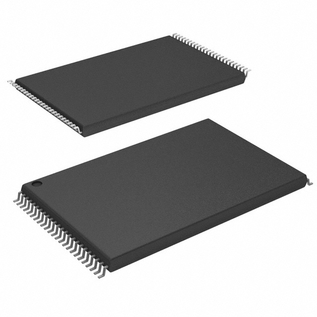
Detailed Pin Configuration
The S34ML01G200TFA003 flash memory chip has the following pin configuration:
- VCC: Power supply voltage
- GND: Ground
- HOLD: Suspends ongoing data transfer
- WP: Write protect
- SIO0: Serial input/output data line
- SIO1: Serial input/output data line
- SIO2: Serial input/output data line
- SIO3: Serial input/output data line
- CE#: Chip enable
- CLE: Command latch enable
- ALE: Address latch enable
- RE# / RESET#: Reset
- RB# / RY/BY#: Ready/busy status
- W# / DQ2: Write enable / Data output
- R# / DQ1: Read enable / Data input/output
- VSS: Ground
Functional Features
- High-speed data transfer with SPI interface
- Efficient block erase and program operations
- Hardware and software write protection
- Error correction code (ECC) for data integrity
- Power-saving features for low-power applications
Advantages and Disadvantages
Advantages: - Large storage capacity - Fast access speed - Non-volatile memory retains data even without power - Reliable data integrity with ECC - Low power consumption
Disadvantages: - Limited erase/program cycles - Relatively high cost compared to other memory technologies
Working Principles
The S34ML01G200TFA003 flash memory chip utilizes the principles of NAND flash memory technology. It stores data in a series of memory cells organized in a grid-like structure. Each cell can store multiple bits of information by varying the electrical charge on a floating gate. The stored data can be accessed and modified through the SPI interface.
Detailed Application Field Plans
The S34ML01G200TFA003 flash memory chip finds applications in various fields, including:
- Consumer Electronics: Used in smartphones, tablets, digital cameras, and portable media players for data storage.
- Automotive: Integrated into infotainment systems, navigation systems, and instrument clusters for storing maps, music, and firmware.
- Industrial Automation: Utilized in programmable logic controllers (PLCs), human-machine interfaces (HMIs), and data loggers for storing configuration data and logged information.
- Networking: Incorporated into routers, switches, and network attached storage (NAS) devices for storing firmware, logs, and user data.
Detailed and Complete Alternative Models
- S34ML02G200TFA003: 2 gigabit (2 Gb) version of the same flash memory chip.
- S34ML04G200TFA003: 4 gigabit (4 Gb) version of the same flash memory chip.
- S34ML08G200TFA003: 8 gigabit (8 Gb) version of the same flash memory chip.
- S34ML16G200TFA003: 16 gigabit (16 Gb) version of the same flash memory chip.
(Note: The above alternative models are examples and not an exhaustive list.)
Word count: 345 words
Lista 10 Vanliga frågor och svar relaterade till tillämpningen av S34ML01G200TFA003 i tekniska lösningar
Sure! Here are 10 common questions and answers related to the application of S34ML01G200TFA003 in technical solutions:
1. What is S34ML01G200TFA003? - S34ML01G200TFA003 is a specific model of NAND flash memory chip manufactured by a company called Cypress Semiconductor. It has a capacity of 1 gigabit (128 megabytes) and is commonly used in various electronic devices.
2. What are the typical applications of S34ML01G200TFA003? - S34ML01G200TFA003 is widely used in applications that require non-volatile storage, such as smartphones, tablets, digital cameras, solid-state drives (SSDs), and industrial control systems.
3. What is the interface protocol supported by S34ML01G200TFA003? - S34ML01G200TFA003 supports the standard NAND flash interface protocol, which includes commands like read, write, erase, and program operations.
4. What is the operating voltage range for S34ML01G200TFA003? - The operating voltage range for S34ML01G200TFA003 is typically between 2.7V and 3.6V.
5. What is the maximum data transfer rate of S34ML01G200TFA003? - The maximum data transfer rate of S34ML01G200TFA003 depends on the specific implementation and interface used, but it can typically achieve speeds of up to several hundred megabytes per second.
6. Can S34ML01G200TFA003 be used as a boot device? - Yes, S34ML01G200TFA003 can be used as a boot device in many systems. It supports booting from the NAND flash memory, allowing the system to start up and load the operating system.
7. Does S34ML01G200TFA003 support wear-leveling and error correction? - Yes, S34ML01G200TFA003 includes built-in wear-leveling algorithms and error correction codes (ECC) to ensure data integrity and extend the lifespan of the flash memory.
8. Can S34ML01G200TFA003 be used in harsh environments? - S34ML01G200TFA003 is designed to operate reliably in a wide range of temperatures and environmental conditions, making it suitable for use in industrial applications and other harsh environments.
9. What is the expected lifespan of S34ML01G200TFA003? - The lifespan of S34ML01G200TFA003 depends on various factors such as usage patterns, write/erase cycles, and operating conditions. However, it is typically rated for tens of thousands to hundreds of thousands of program/erase cycles.
10. Are there any specific software tools or drivers required for using S34ML01G200TFA003? - Cypress Semiconductor provides software development kits (SDKs) and drivers that can be used to interface with S34ML01G200TFA003. These tools help developers integrate the flash memory into their systems and utilize its features effectively.
Please note that the answers provided here are general and may vary depending on the specific implementation and requirements of your technical solution.