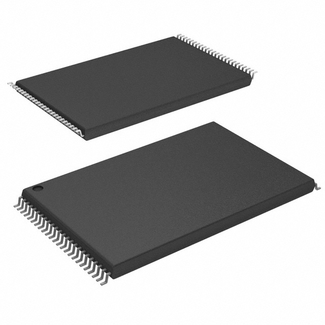
S34ML01G200TFB003
Product Overview
Category
S34ML01G200TFB003 belongs to the category of NAND flash memory.
Use
It is primarily used for data storage in various electronic devices such as smartphones, tablets, digital cameras, and solid-state drives (SSDs).
Characteristics
- High storage capacity: S34ML01G200TFB003 has a storage capacity of 1 gigabit (1 Gb).
- Fast data transfer rate: It offers high-speed data transfer, allowing for quick read and write operations.
- Reliable performance: The product ensures reliable data storage and retrieval, minimizing the risk of data loss.
- Low power consumption: S34ML01G200TFB003 is designed to consume minimal power, making it suitable for battery-powered devices.
- Compact package: It comes in a compact form factor, enabling easy integration into various electronic devices.
Package and Quantity
S34ML01G200TFB003 is packaged in a small outline integrated circuit (SOIC) package. Each package contains one unit of the product.
Specifications
- Storage Capacity: 1 Gb
- Interface: NAND Flash
- Supply Voltage: 2.7V - 3.6V
- Operating Temperature Range: -40°C to +85°C
- Data Transfer Rate: Up to 200 Mbps (Megabits per second)
- Erase/Program Cycles: Up to 100,000 cycles
Detailed Pin Configuration
The pin configuration of S34ML01G200TFB003 is as follows:
| Pin Number | Pin Name | Description | |------------|----------|-------------| | 1 | VCC | Power supply voltage | | 2 | GND | Ground | | 3 | CE# | Chip Enable | | 4 | CLE | Command Latch Enable | | 5 | ALE | Address Latch Enable | | 6-13 | A0-A7 | Address Inputs | | 14 | RE# | Read Enable | | 15 | WE# | Write Enable | | 16-23 | DQ0-DQ7 | Data Inputs/Outputs | | 24 | R/B# | Ready/Busy Status |
Functional Features
- Block Erase: S34ML01G200TFB003 allows for erasing data in large blocks, enhancing efficiency.
- Page Program: It supports fast page programming, enabling quick data writing.
- Random Access: The product provides random access to individual memory cells, facilitating efficient data retrieval.
- Error Correction Code (ECC): S34ML01G200TFB003 incorporates ECC algorithms to ensure data integrity and reliability.
Advantages and Disadvantages
Advantages
- High storage capacity
- Fast data transfer rate
- Reliable performance
- Low power consumption
- Compact form factor
Disadvantages
- Limited erase/program cycles
- Relatively higher cost compared to other memory technologies
Working Principles
S34ML01G200TFB003 utilizes NAND flash memory technology. It stores data by trapping electrons in a floating gate within each memory cell. When a voltage is applied, the trapped electrons determine the stored data. Reading involves sensing the presence or absence of charge in the memory cells.
Detailed Application Field Plans
S34ML01G200TFB003 finds applications in various electronic devices, including: 1. Smartphones and tablets for storing user data, apps, and operating systems. 2. Digital cameras for storing high-resolution photos and videos. 3. Solid-state drives (SSDs) for fast and reliable data storage in computers and servers. 4. Portable media players for storing music, videos, and other multimedia content.
Detailed and Complete Alternative Models
- S34ML02G200TFB003: A similar NAND flash memory with double the storage capacity (2 Gb).
- S34ML04G200TFB003: A higher-capacity alternative with 4 Gb of storage.
- S34ML08G200TFB003: Offers even greater storage capacity with 8 Gb.
These alternative models provide options for different storage requirements in electronic devices.
Word count: 511 words
Lista 10 Vanliga frågor och svar relaterade till tillämpningen av S34ML01G200TFB003 i tekniska lösningar
Sure! Here are 10 common questions and answers related to the application of S34ML01G200TFB003 in technical solutions:
Q: What is S34ML01G200TFB003? A: S34ML01G200TFB003 is a specific model of NAND flash memory chip manufactured by a company called Cypress Semiconductor.
Q: What are the key features of S34ML01G200TFB003? A: Some key features of S34ML01G200TFB003 include a storage capacity of 1GB, a high-speed interface, and advanced error correction capabilities.
Q: In what types of technical solutions can S34ML01G200TFB003 be used? A: S34ML01G200TFB003 can be used in various applications such as embedded systems, automotive electronics, industrial control systems, and consumer electronics.
Q: How does S34ML01G200TFB003 connect to other components in a system? A: S34ML01G200TFB003 typically connects to a system using a standard NAND flash interface, such as the Open NAND Flash Interface (ONFI) or Toggle Mode.
Q: What is the maximum data transfer rate supported by S34ML01G200TFB003? A: S34ML01G200TFB003 supports a maximum data transfer rate of up to 200 megabytes per second (MB/s).
Q: Can S34ML01G200TFB003 withstand harsh environmental conditions? A: Yes, S34ML01G200TFB003 is designed to operate reliably in a wide range of temperatures and can withstand shock and vibration.
Q: Does S34ML01G200TFB003 support wear-leveling algorithms? A: Yes, S34ML01G200TFB003 supports wear-leveling algorithms to distribute write operations evenly across the memory cells, extending its lifespan.
Q: Can S34ML01G200TFB003 be used for code execution in microcontrollers? A: Yes, S34ML01G200TFB003 can be used for code execution in microcontrollers by connecting it to the appropriate interface and configuring the system accordingly.
Q: What is the power consumption of S34ML01G200TFB003 during operation? A: The power consumption of S34ML01G200TFB003 varies depending on the specific operation but is generally low compared to other storage solutions.
Q: Are there any specific software requirements for using S34ML01G200TFB003? A: S34ML01G200TFB003 is compatible with various operating systems and file systems, so there are no specific software requirements, but drivers may be needed for proper integration.
Please note that these answers are general and may vary based on the specific implementation and requirements of a technical solution.


