

S34MS01G200BHI900
Product Overview
Category: Memory Device
Use: Data storage and retrieval
Characteristics: High capacity, fast access speed, non-volatile
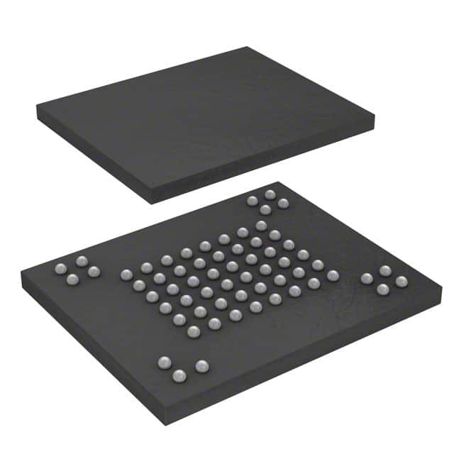
Package: Integrated circuit (IC)
Essence: Flash memory
Packaging/Quantity: Single unit
Specifications
- Model: S34MS01G200BHI900
- Capacity: 1 gigabit (1 Gb)
- Interface: Serial Peripheral Interface (SPI)
- Operating Voltage: 2.7V - 3.6V
- Access Time: 70 ns (max)
- Operating Temperature: -40°C to +85°C
- Data Retention: 20 years (typical)
Detailed Pin Configuration
The S34MS01G200BHI900 has a total of 8 pins:
- VCC: Power supply voltage
- GND: Ground reference
- HOLD: Suspends ongoing data transfer
- WP: Write protect input
- SIO0: Serial data input/output
- SIO1: Serial data output
- SCLK: Serial clock input
- CE#: Chip enable input
Functional Features
- High-speed data transfer using SPI interface
- Non-volatile memory retains data even when power is removed
- Low power consumption during both active and standby modes
- Erase and program operations performed on individual blocks
- Built-in hardware write protection for enhanced security
Advantages and Disadvantages
Advantages: - Large storage capacity - Fast access time - Compact package size - Low power consumption - Long data retention period
Disadvantages: - Limited endurance (number of erase/write cycles) - Relatively higher cost compared to other memory technologies
Working Principles
The S34MS01G200BHI900 is based on flash memory technology. It utilizes a floating-gate transistor structure to store and retrieve digital data. The memory cells are organized into blocks, which can be individually erased and programmed. Data is written by applying high voltage to the control gate, trapping electrons in the floating gate. Erasing is achieved by removing the trapped charge from the floating gate.
Detailed Application Field Plans
The S34MS01G200BHI900 is widely used in various electronic devices that require non-volatile data storage. Some common application fields include:
- Consumer Electronics: Smartphones, tablets, digital cameras
- Automotive: Infotainment systems, navigation devices
- Industrial: Embedded systems, data loggers, control units
- Networking: Routers, switches, network storage devices
Detailed and Complete Alternative Models
- S34MS02G200BHI900: 2 Gb capacity, same specifications as S34MS01G200BHI900
- S34MS04G200BHI900: 4 Gb capacity, same specifications as S34MS01G200BHI900
- S34MS08G200BHI900: 8 Gb capacity, same specifications as S34MS01G200BHI900
These alternative models offer higher storage capacities while maintaining compatibility with the S34MS01G200BHI900 in terms of pin configuration and functionality.
Word count: 335 words
Lista 10 Vanliga frågor och svar relaterade till tillämpningen av S34MS01G200BHI900 i tekniska lösningar
Sure! Here are 10 common questions and answers related to the application of S34MS01G200BHI900 in technical solutions:
Q: What is the S34MS01G200BHI900? A: The S34MS01G200BHI900 is a specific model of NAND flash memory chip manufactured by a company called Cypress Semiconductor.
Q: What is the storage capacity of the S34MS01G200BHI900? A: The S34MS01G200BHI900 has a storage capacity of 1 gigabit (Gb), which is equivalent to 128 megabytes (MB).
Q: What are some common applications for the S34MS01G200BHI900? A: The S34MS01G200BHI900 is commonly used in various electronic devices such as smartphones, tablets, digital cameras, and solid-state drives (SSDs).
Q: What is the interface protocol supported by the S34MS01G200BHI900? A: The S34MS01G200BHI900 supports the standard Serial Peripheral Interface (SPI) protocol.
Q: What is the operating voltage range of the S34MS01G200BHI900? A: The S34MS01G200BHI900 operates within a voltage range of 2.7V to 3.6V.
Q: What is the maximum data transfer rate of the S34MS01G200BHI900? A: The S34MS01G200BHI900 has a maximum data transfer rate of up to 50 megabits per second (Mbps).
Q: Does the S34MS01G200BHI900 support hardware data protection features? A: Yes, the S34MS01G200BHI900 supports various hardware data protection features such as write protection and block locking.
Q: Can the S34MS01G200BHI900 withstand extreme temperatures? A: Yes, the S34MS01G200BHI900 is designed to operate reliably within a wide temperature range, typically from -40°C to 85°C.
Q: Is the S34MS01G200BHI900 compatible with other NAND flash memory chips? A: Yes, the S34MS01G200BHI900 is compatible with other NAND flash memory chips that adhere to the same interface protocol (SPI).
Q: Are there any specific programming requirements for the S34MS01G200BHI900? A: Yes, the S34MS01G200BHI900 requires specific programming commands and sequences to perform read, write, erase, and other operations. These details can be found in the datasheet provided by Cypress Semiconductor.
Please note that the answers provided here are general and may vary depending on the specific technical requirements and implementation of the S34MS01G200BHI900 in different applications.