

54FCT240ATDB
Product Overview
Category: Integrated Circuit (IC)
Use: The 54FCT240ATDB is a high-speed octal buffer/line driver designed for general-purpose applications. It is commonly used in digital systems to provide buffering and signal amplification capabilities.
Characteristics: - High-speed operation - Low power consumption - Wide operating voltage range - Schmitt trigger inputs for noise immunity - TTL-compatible input and output levels
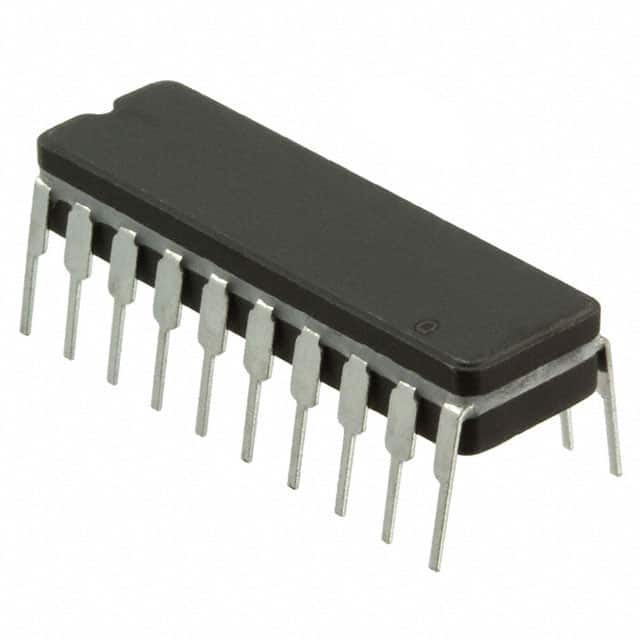
Package: The 54FCT240ATDB is available in a standard 20-pin dual in-line package (DIP), which provides ease of use and compatibility with various circuit boards.
Essence: This IC serves as a crucial component in digital systems, ensuring reliable signal transmission and driving capability.
Packaging/Quantity: The 54FCT240ATDB is typically packaged in reels or tubes, containing a quantity of 25 or 50 units per package.
Specifications
- Supply Voltage Range: 4.5V to 5.5V
- Input Voltage Range: 0V to Vcc
- Output Voltage Range: 0V to Vcc
- Operating Temperature Range: -40°C to +85°C
- Propagation Delay Time: 3.5ns (typical)
- Output Drive Capability: ±24mA
Pin Configuration
The 54FCT240ATDB features a 20-pin DIP package with the following pin configuration:
+---+--+---+
   A1 -|1  +--+ 20|- Vcc
   A2 -|2         |- B1
   A3 -|3         |- B2
   A4 -|4         |- B3
   A5 -|5         |- B4
   A6 -|6         |- B5
   A7 -|7         |- B6
   A8 -|8         |- B7
  GND -|9         |- B8
  OE  -|10        |- Y1
  Y2  -|11        |- Y3
  Y4  -|12        |- Y5
  Y6  -|13        |- Y7
  Y8  -|14        |- OE#
  B8  -|15        |- GND
  B7  -|16        |- A8
  B6  -|17        |- A7
  B5  -|18        |- A6
  B4  -|19        |- A5
  B3  -|20        |- A4
       +---+--+---+
Functional Features
- Octal buffer/line driver with 3-state outputs
- Provides non-inverting buffering of inputs
- Capable of driving both standard and open-collector outputs
- Output enable (OE) input allows for tri-state operation, enabling multiple devices to share a common bus
Advantages and Disadvantages
Advantages: - High-speed operation enables efficient signal transmission - Low power consumption contributes to energy efficiency - Wide operating voltage range enhances compatibility with various systems - Schmitt trigger inputs provide noise immunity, ensuring reliable performance - TTL-compatible levels facilitate integration with existing digital circuits
Disadvantages: - Limited output drive capability may not be suitable for high-current applications - Propagation delay time may introduce timing issues in certain scenarios
Working Principles
The 54FCT240ATDB operates by receiving input signals on the A1-A8 pins. These signals are buffered and amplified internally before being transmitted to the corresponding Y1-Y8 output pins. The output enable (OE) input controls the tri-state operation, allowing the outputs to be either active or in a high-impedance state.
Detailed Application Field Plans
The 54FCT240ATDB finds applications in various digital systems, including but not limited to: - Microprocessors and microcontrollers - Memory systems - Data communication equipment - Industrial automation systems - Test and measurement instruments
Alternative Models
For similar functionality and compatibility, alternative models to the 54FCT240ATDB include: - SN74F240 - Texas Instruments - MC74F240 - ON Semiconductor - CD54FCT240 - Texas Instruments - HD74F240 - Renesas Electronics
These alternative models offer comparable features and can be used as substitutes based on specific requirements.
Word count: 529 words
Lista 10 Vanliga frågor och svar relaterade till tillämpningen av 54FCT240ATDB i tekniska lösningar
Sure! Here are 10 common questions and answers related to the application of 54FCT240ATDB in technical solutions:
Q: What is the 54FCT240ATDB? A: The 54FCT240ATDB is a octal buffer/line driver with 3-state outputs, commonly used in digital logic circuits.
Q: What is the maximum operating voltage for the 54FCT240ATDB? A: The maximum operating voltage for the 54FCT240ATDB is typically 5V.
Q: How many inputs and outputs does the 54FCT240ATDB have? A: The 54FCT240ATDB has 8 inputs and 8 outputs.
Q: Can the 54FCT240ATDB be used as a level shifter? A: Yes, the 54FCT240ATDB can be used as a level shifter to convert signals between different voltage levels.
Q: What is the maximum output current that the 54FCT240ATDB can drive? A: The 54FCT240ATDB can typically drive up to 24mA of output current.
Q: Is the 54FCT240ATDB compatible with TTL logic levels? A: Yes, the 54FCT240ATDB is compatible with TTL logic levels, making it suitable for interfacing with TTL devices.
Q: Can the 54FCT240ATDB be used in high-speed applications? A: Yes, the 54FCT240ATDB is designed for high-speed operation and can be used in applications with fast switching requirements.
Q: Does the 54FCT240ATDB have internal pull-up or pull-down resistors? A: No, the 54FCT240ATDB does not have internal pull-up or pull-down resistors. External resistors may be required for proper operation.
Q: Can the 54FCT240ATDB be used in bidirectional applications? A: No, the 54FCT240ATDB is a unidirectional buffer and cannot be used for bidirectional communication.
Q: What is the power supply voltage range for the 54FCT240ATDB? A: The power supply voltage range for the 54FCT240ATDB is typically between 4.5V and 5.5V.