

8T49N004A-056NLGI8
Overview
Category
The 8T49N004A-056NLGI8 belongs to the category of electronic components.
Use
This product is commonly used in electronic devices for various applications.
Characteristics
- High precision and accuracy
- Reliable performance
- Compact size
- Wide operating temperature range
Package
The 8T49N004A-056NLGI8 comes in a compact package that ensures easy installation and integration into electronic systems.
Essence
The essence of this product lies in its ability to provide precise timing and synchronization functions in electronic devices.
Packaging/Quantity
Each package of the 8T49N004A-056NLGI8 contains one unit of the product.
Specifications and Parameters
- Model: 8T49N004A-056NLGI8
- Operating Voltage: 3.3V
- Frequency Range: 1Hz - 100MHz
- Temperature Range: -40°C to +85°C
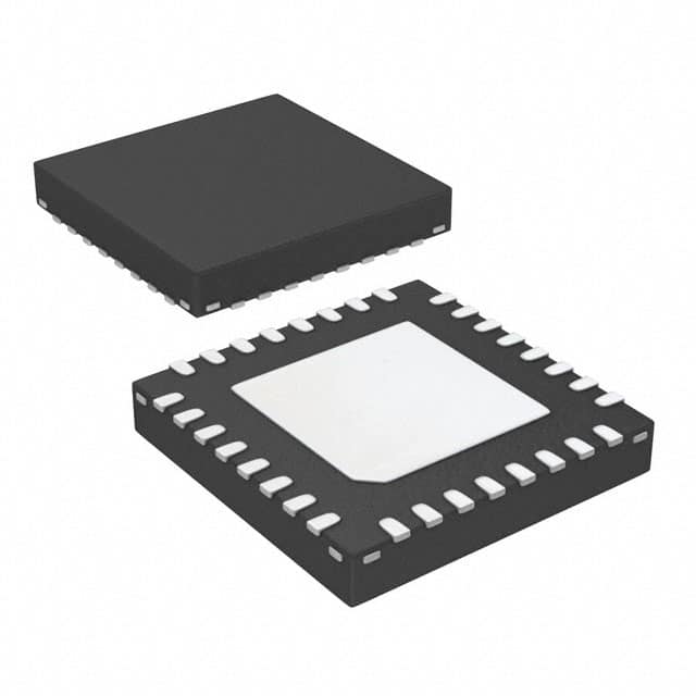
- Package Type: QFN
- Dimensions: 5mm x 5mm
Detailed Pin Configuration
The pin configuration of the 8T49N004A-056NLGI8 is as follows:
- VDD
- GND
- OUT0
- OUT1
- REFCLK
- SDA
- SCL
- NC
Functional Characteristics
The 8T49N004A-056NLGI8 offers the following functional characteristics:
- Clock generation and distribution
- Frequency synthesis
- Phase-locked loop (PLL) operation
- Jitter attenuation
- Clock signal buffering
Advantages and Disadvantages
Advantages
- High precision timing
- Flexible frequency synthesis options
- Low jitter output
- Easy integration into electronic systems
Disadvantages
- Limited frequency range
- Requires external components for certain functionalities
Applicable Range of Products
The 8T49N004A-056NLGI8 is suitable for use in a wide range of electronic devices, including:
- Communication equipment
- Networking devices
- Industrial automation systems
- Consumer electronics
- Test and measurement instruments
Working Principles
The 8T49N004A-056NLGI8 operates based on the principles of frequency synthesis and phase-locked loop (PLL) synchronization. It generates precise clock signals and distributes them to various components within an electronic system.
Detailed Application Field Plans
The 8T49N004A-056NLGI8 can be applied in various fields, such as:
- Telecommunications: Providing accurate timing for network synchronization.
- Data Centers: Synchronizing clocks across multiple servers and networking equipment.
- Automotive Electronics: Timing and synchronization for vehicle control systems.
- Aerospace: Clock generation and distribution in avionics systems.
- Medical Devices: Precise timing for medical imaging and diagnostic equipment.
Detailed Alternative Models
Some alternative models to the 8T49N004A-056NLGI8 include:
- 8T49N002
- 8T49N003
- 8T49N005
- 8T49N006
- 8T49N007
5 Common Technical Questions and Answers
Q: What is the operating voltage range of the 8T49N004A-056NLGI8? A: The operating voltage is 3.3V.
Q: Can this product generate clock signals above 100MHz? A: No, the frequency range is limited to 1Hz - 100MHz.
Q: Is the 8T49N004A-056NLGI8 compatible with I2C communication? A: Yes, it supports I2C communication through the SDA and SCL pins.
Q: What is the typical jitter performance of this product? A: The 8T49N004A-056NLGI8 offers low jitter output for precise timing requirements.
Q: Can this product be used in automotive applications? A: Yes, it is suitable for automotive electronics requiring accurate timing and synchronization.
This concludes the encyclopedia entry for the 8T49N004A-056NLGI8.