

IPD50R650CEATMA1
Introduction
The IPD50R650CEATMA1 is a power MOSFET belonging to the category of electronic components. It is widely used in various applications due to its unique characteristics and functional features. This entry provides an overview of the product, including its basic information, specifications, detailed pin configuration, functional features, advantages and disadvantages, working principles, application field plans, and alternative models.
Basic Information Overview
- Category: Electronic Components
- Use: Power MOSFET for electronic circuits
- Characteristics: High power handling capacity, low on-resistance, fast switching speed
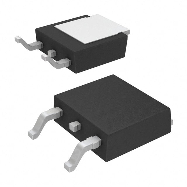
- Package: TO-252-3 (DPAK)
- Essence: Efficient power management and control
- Packaging/Quantity: Typically packaged in reels or tubes, quantity varies based on supplier
Specifications
- Voltage Rating: 650V
- Current Rating: 50A
- On-Resistance: Low RDS(on) value
- Operating Temperature Range: -55°C to 150°C
- Gate-Source Voltage (Max): ±20V
- Package Type: TO-252-3 (DPAK)
Detailed Pin Configuration
The IPD50R650CEATMA1 follows the standard pin configuration for a TO-252-3 (DPAK) package: 1. Source (S) 2. Gate (G) 3. Drain (D)
Functional Features
- High Power Handling: Capable of handling high currents and voltages
- Low On-Resistance: Minimizes power loss and heat generation
- Fast Switching Speed: Enables efficient control in switching applications
- Enhanced Thermal Performance: Designed for effective heat dissipation
Advantages and Disadvantages
Advantages
- High power handling capacity
- Low on-resistance for improved efficiency
- Fast switching speed for responsive control
- Enhanced thermal performance for reliability
Disadvantages
- Sensitive to static discharge, requiring proper handling
- Higher cost compared to standard MOSFETs
Working Principles
The IPD50R650CEATMA1 operates based on the principles of field-effect transistors, utilizing the voltage applied to the gate terminal to control the flow of current between the source and drain terminals. When the gate-source voltage reaches the threshold, the MOSFET switches on, allowing current to flow through.
Detailed Application Field Plans
The IPD50R650CEATMA1 finds extensive use in various applications, including: - Switching power supplies - Motor control systems - Inverters and converters - LED lighting drivers - Audio amplifiers - Automotive electronics
Detailed and Complete Alternative Models
- IPD50R650CE: Similar specifications with minor variations
- IPD50R650CEC: Enhanced thermal performance variant
- IPD50R650CEX: Extended temperature range version
In conclusion, the IPD50R650CEATMA1 is a versatile power MOSFET with high power handling capacity, low on-resistance, and fast switching speed, making it suitable for diverse electronic applications. Its functional features, advantages, and working principles contribute to its widespread use in various fields, while alternative models provide flexibility in design and application.
Word Count: 443
Lista 10 Vanliga frågor och svar relaterade till tillämpningen av IPD50R650CEATMA1 i tekniska lösningar
What is the maximum drain current of IPD50R650CEATMA1?
- The maximum drain current of IPD50R650CEATMA1 is 25A.
What is the typical on-state resistance of IPD50R650CEATMA1?
- The typical on-state resistance of IPD50R650CEATMA1 is 65mΩ.
What is the voltage rating of IPD50R650CEATMA1?
- IPD50R650CEATMA1 has a voltage rating of 650V.
What type of package does IPD50R650CEATMA1 come in?
- IPD50R650CEATMA1 comes in a TO-252-3 package.
What are the typical applications for IPD50R650CEATMA1?
- IPD50R650CEATMA1 is commonly used in motor control, power supplies, and lighting applications.
What is the gate charge of IPD50R650CEATMA1?
- The gate charge of IPD50R650CEATMA1 is typically 18nC.
Does IPD50R650CEATMA1 have built-in protection features?
- Yes, IPD50R650CEATMA1 has built-in overcurrent and overtemperature protection.
What is the operating temperature range of IPD50R650CEATMA1?
- IPD50R650CEATMA1 has an operating temperature range of -55°C to 150°C.
Is IPD50R650CEATMA1 RoHS compliant?
- Yes, IPD50R650CEATMA1 is RoHS compliant.
Can IPD50R650CEATMA1 be used in high-frequency switching applications?
- Yes, IPD50R650CEATMA1 is suitable for high-frequency switching due to its low on-state resistance and fast switching characteristics.