

IPP65R190E6XKSA1
Product Overview
- Category: Power MOSFET
- Use: Power switching applications
- Characteristics: High voltage, low on-resistance, fast switching speed
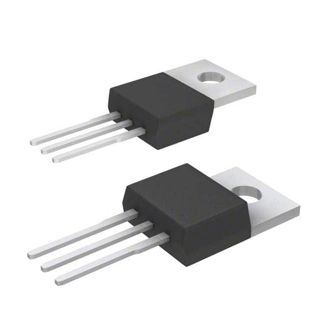
- Package: TO-220
- Essence: Efficient power management
- Packaging/Quantity: Tube/50 pieces
Specifications
- Voltage Rating: 650V
- Current Rating: 32A
- On-Resistance: 190mΩ
- Gate Charge: 38nC
- Operating Temperature: -55°C to 175°C
Detailed Pin Configuration
The IPP65R190E6XKSA1 follows the standard pin configuration for a TO-220 package: 1. Gate (G) 2. Drain (D) 3. Source (S)
Functional Features
- Low gate charge for fast switching
- Low on-resistance for high efficiency
- Avalanche energy specified
- Enhanced ESD protection
Advantages and Disadvantages
Advantages
- High voltage rating
- Low on-resistance
- Fast switching speed
- Enhanced ESD protection
Disadvantages
- Higher gate charge compared to some alternatives
- Limited operating temperature range
Working Principles
The IPP65R190E6XKSA1 operates based on the principles of metal-oxide-semiconductor field-effect transistors (MOSFETs), utilizing its high voltage capability and low on-resistance to efficiently switch power in various applications.
Detailed Application Field Plans
The IPP65R190E6XKSA1 is suitable for a wide range of power switching applications, including but not limited to: - Switch mode power supplies - Motor control - Inverters - DC-DC converters
Detailed and Complete Alternative Models
Some alternative models to the IPP65R190E6XKSA1 include: - IPP60R190E6 - IPP65R190CFD - IPP65R190C7
This completes the entry for IPP65R190E6XKSA1, providing comprehensive information about its category, use, characteristics, specifications, pin configuration, functional features, advantages and disadvantages, working principles, application field plans, and alternative models.
Lista 10 Vanliga frågor och svar relaterade till tillämpningen av IPP65R190E6XKSA1 i tekniska lösningar
What is the maximum drain current of IPP65R190E6XKSA1?
- The maximum drain current of IPP65R190E6XKSA1 is 65A.
What is the typical gate charge of IPP65R190E6XKSA1?
- The typical gate charge of IPP65R190E6XKSA1 is 45nC.
What is the voltage rating of IPP65R190E6XKSA1?
- IPP65R190E6XKSA1 has a voltage rating of 650V.
What are the typical applications for IPP65R190E6XKSA1?
- IPP65R190E6XKSA1 is commonly used in applications such as motor control, power supplies, and inverters.
What is the on-state resistance of IPP65R190E6XKSA1?
- The on-state resistance of IPP65R190E6XKSA1 is typically 0.19 ohms.
Does IPP65R190E6XKSA1 have built-in protection features?
- Yes, IPP65R190E6XKSA1 includes built-in protection features such as overcurrent protection and thermal shutdown.
What is the operating temperature range of IPP65R190E6XKSA1?
- IPP65R190E6XKSA1 has an operating temperature range of -55°C to 150°C.
Is IPP65R190E6XKSA1 suitable for high-frequency switching applications?
- Yes, IPP65R190E6XKSA1 is suitable for high-frequency switching due to its low gate charge and fast switching characteristics.
Can IPP65R190E6XKSA1 be used in automotive applications?
- Yes, IPP65R190E6XKSA1 is qualified for automotive applications and meets relevant industry standards.
What are the key advantages of using IPP65R190E6XKSA1 in technical solutions?
- The key advantages of IPP65R190E6XKSA1 include high current capability, low on-state resistance, and robust protection features, making it suitable for demanding technical solutions.