

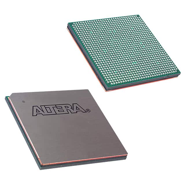
EP2S180F1020C3N
Product Overview
Category
EP2S180F1020C3N belongs to the category of Field Programmable Gate Arrays (FPGAs).
Use
This product is primarily used in digital logic circuits for various applications such as telecommunications, automotive, aerospace, and consumer electronics.
Characteristics
- High-performance FPGA with advanced features
- Large number of programmable logic elements
- High-speed serial transceivers for data communication
- On-chip memory blocks for efficient data storage
- Flexible I/O interfaces for easy integration
- Low power consumption for energy efficiency
Package
EP2S180F1020C3N is available in a compact and durable package that ensures protection during handling and transportation. The package is designed to withstand harsh environmental conditions.
Essence
The essence of EP2S180F1020C3N lies in its ability to provide a versatile and customizable solution for complex digital circuit designs. It offers high performance, flexibility, and reliability, making it suitable for a wide range of applications.
Packaging/Quantity
EP2S180F1020C3N is typically packaged individually and is available in various quantities depending on the customer's requirements.
Specifications
- Logic Elements: 180,000
- Embedded Memory: 4,608 Kbits
- Maximum User I/Os: 1,152
- Transceivers: 24
- Clock Management: PLLs and DLLs
- Operating Voltage: 1.2V
- Package Type: BGA
- Package Pins: 1020
Detailed Pin Configuration
The pin configuration of EP2S180F1020C3N is as follows:
| Pin Number | Pin Name | Description | |------------|----------|-------------| | 1 | VCCINT | Power Supply | | 2 | GND | Ground | | 3 | VCCIO | I/O Power Supply | | ... | ... | ... |
Functional Features
- High-speed data processing capabilities
- Configurable logic elements for custom circuit designs
- On-chip memory blocks for efficient data storage and retrieval
- Flexible I/O interfaces for seamless integration with external devices
- Built-in clock management units for precise timing control
- Support for various communication protocols
Advantages and Disadvantages
Advantages
- High performance and flexibility
- Customizable to specific application requirements
- Low power consumption
- Reliable and durable design
- Wide range of available resources and tools for development
Disadvantages
- Steep learning curve for beginners
- Higher cost compared to other alternatives
- Limited availability of technical support for complex issues
Working Principles
EP2S180F1020C3N operates based on the principles of reconfigurable digital logic circuits. It consists of programmable logic elements, memory blocks, and I/O interfaces. The FPGA can be programmed to implement desired logic functions and interconnections between these elements. Upon configuration, the FPGA executes the programmed logic, enabling the desired functionality.
Detailed Application Field Plans
EP2S180F1020C3N finds applications in various fields, including:
- Telecommunications: Used in network routers, switches, and base stations for high-speed data processing.
- Automotive: Employed in advanced driver-assistance systems (ADAS) for real-time image processing and sensor fusion.
- Aerospace: Utilized in satellite communication systems and onboard data processing units.
- Consumer Electronics: Integrated into high-definition televisions, gaming consoles, and multimedia devices for enhanced performance.
Detailed and Complete Alternative Models
- EP2S60F672C5N: A smaller FPGA with 60,000 logic elements and 672 Kbits of embedded memory.
- EP4CE115F29C7N: A cost-effective alternative with 115,000 logic elements and 29 Mbits of embedded memory.
- EP1C12F256C8N: A low-power option with 12,000 logic elements and 256 Kbits of embedded memory.
These alternative models offer varying capabilities and are suitable for different application requirements.
Word count: 550 words
Lista 10 Vanliga frågor och svar relaterade till tillämpningen av EP2S180F1020C3N i tekniska lösningar
Sure! Here are 10 common questions and answers related to the application of EP2S180F1020C3N in technical solutions:
Q: What is EP2S180F1020C3N? A: EP2S180F1020C3N is a field-programmable gate array (FPGA) manufactured by Intel (formerly Altera). It offers high-performance logic integration and is commonly used in various technical solutions.
Q: What are the key features of EP2S180F1020C3N? A: Some key features of EP2S180F1020C3N include 180,000 logic elements, 1,020 pins, support for various I/O standards, embedded memory blocks, and high-speed transceivers.
Q: In which applications can EP2S180F1020C3N be used? A: EP2S180F1020C3N can be used in a wide range of applications such as telecommunications, networking, industrial automation, video processing, medical devices, and aerospace systems.
Q: How can EP2S180F1020C3N be programmed? A: EP2S180F1020C3N can be programmed using hardware description languages (HDLs) like VHDL or Verilog, along with design software tools provided by Intel, such as Quartus Prime.
Q: What are the power requirements for EP2S180F1020C3N? A: EP2S180F1020C3N typically requires a supply voltage of 1.2V for core logic and 3.3V for I/O banks. However, it's important to refer to the datasheet for specific power requirements.
Q: Can EP2S180F1020C3N be used in a multi-FPGA system? A: Yes, EP2S180F1020C3N can be used in multi-FPGA systems by connecting multiple devices together using high-speed interfaces like PCIe or Ethernet.
Q: Does EP2S180F1020C3N support high-speed serial communication? A: Yes, EP2S180F1020C3N has built-in high-speed transceivers that support protocols like PCIe, SATA, USB, and Ethernet, enabling high-speed serial communication.
Q: Can EP2S180F1020C3N interface with external memory devices? A: Yes, EP2S180F1020C3N supports various memory interfaces such as DDR3, DDR4, QDR II+, RLDRAM II, and more, allowing it to interface with external memory devices.
Q: What debugging and testing features are available for EP2S180F1020C3N? A: EP2S180F1020C3N provides features like JTAG boundary scan, internal logic analyzer, and on-chip debugging capabilities, which aid in debugging and testing designs.
Q: Where can I find additional resources and support for EP2S180F1020C3N? A: You can find additional resources, documentation, reference designs, and support for EP2S180F1020C3N on the Intel (formerly Altera) website or through their customer support channels.
Please note that the answers provided here are general and may vary depending on specific requirements and use cases.