

LFE2-70E-7FN672C
Product Overview
Category
The LFE2-70E-7FN672C belongs to the category of Field Programmable Gate Arrays (FPGAs).
Use
This FPGA is commonly used in electronic circuits for various applications, including digital signal processing, telecommunications, and embedded systems.
Characteristics
- High-performance programmable logic device
- Offers flexibility and reconfigurability
- Provides high-speed data processing capabilities
- Supports complex algorithms and computations
- Enables rapid prototyping and development
Package
The LFE2-70E-7FN672C comes in a compact and durable package, ensuring protection against environmental factors such as temperature, humidity, and physical damage.
Essence
The essence of this FPGA lies in its ability to provide a customizable hardware platform that can be programmed to perform specific tasks, replacing traditional fixed-function integrated circuits.
Packaging/Quantity
Each package of LFE2-70E-7FN672C contains one unit of the FPGA.
Specifications
- Model: LFE2-70E-7FN672C
- Logic Elements: 70,000
- Number of I/O Pins: 672
- Operating Voltage: 1.2V
- Maximum Frequency: 500 MHz
- Configuration Memory: 4 Mb
- Embedded Memory: 2,048 Kbits
- Power Consumption: 0.9W
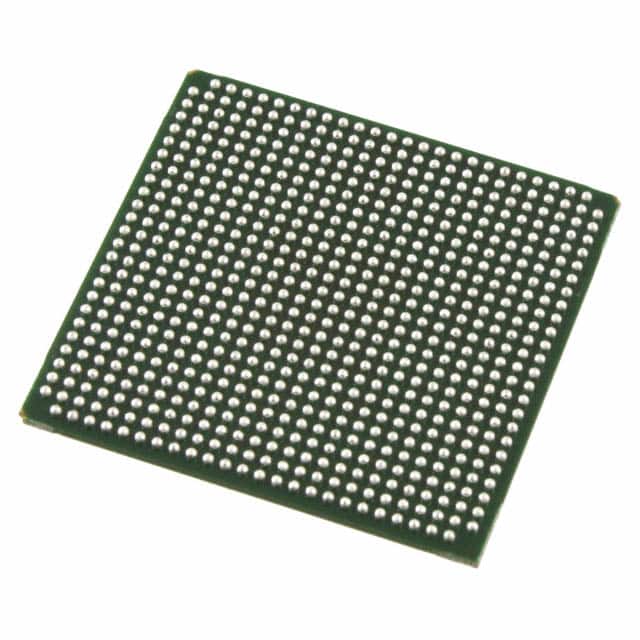
Detailed Pin Configuration
The LFE2-70E-7FN672C has a total of 672 pins, each serving a specific purpose in the circuit design. The pin configuration includes input/output pins, power supply pins, clock pins, and configuration pins. A detailed pin diagram can be found in the product datasheet.
Functional Features
- High-speed data processing capabilities
- Configurable logic elements for custom functionality
- Embedded memory blocks for data storage
- Flexible I/O interfaces for seamless integration with external devices
- Clock management resources for precise timing control
- Built-in configuration memory for easy reprogramming
Advantages and Disadvantages
Advantages
- Flexibility and reconfigurability allow for rapid prototyping and development.
- High-performance capabilities enable complex algorithm implementation.
- Compact package ensures durability and protection against environmental factors.
Disadvantages
- Steeper learning curve compared to traditional fixed-function integrated circuits.
- Higher power consumption compared to some specialized ASICs.
- Limited availability of alternative models due to proprietary nature.
Working Principles
The LFE2-70E-7FN672C operates based on the principles of digital logic design. It consists of configurable logic elements, embedded memory blocks, and I/O interfaces. The FPGA can be programmed using a Hardware Description Language (HDL) to define the desired functionality. Upon programming, the FPGA's internal connections are configured, allowing it to perform the specified tasks.
Detailed Application Field Plans
The LFE2-70E-7FN672C finds applications in various fields, including:
- Digital Signal Processing: Used for real-time audio and video processing, image recognition, and compression algorithms.
- Telecommunications: Employed in network routers, switches, and base stations for high-speed data processing and protocol handling.
- Embedded Systems: Integrated into automotive electronics, industrial control systems, and consumer electronics for custom functionality and performance optimization.
Detailed and Complete Alternative Models
While the LFE2-70E-7FN672C is a highly capable FPGA, there are alternative models available from different manufacturers that offer similar functionalities. Some notable alternatives include:
- Xilinx Virtex UltraScale+: Offers higher logic capacity and advanced features for demanding applications.
- Intel Cyclone V: Provides a cost-effective solution with good performance and power efficiency.
- Microchip PolarFire: Focuses on low-power applications with high-speed data processing capabilities.
These alternative models can be considered based on specific project requirements and budget constraints.
Word count: 527 words
Lista 10 Vanliga frågor och svar relaterade till tillämpningen av LFE2-70E-7FN672C i tekniska lösningar
Sure! Here are 10 common questions and answers related to the application of LFE2-70E-7FN672C in technical solutions:
Q: What is the LFE2-70E-7FN672C? A: The LFE2-70E-7FN672C is a field-programmable gate array (FPGA) manufactured by Lattice Semiconductor.
Q: What are the key features of the LFE2-70E-7FN672C? A: The key features include 70,000 lookup tables (LUTs), 672-pin fine pitch ball grid array (FBGA) package, low power consumption, and high-speed performance.
Q: What are some typical applications for the LFE2-70E-7FN672C? A: The LFE2-70E-7FN672C is commonly used in applications such as telecommunications, industrial automation, automotive electronics, and medical devices.
Q: How can I program the LFE2-70E-7FN672C? A: The LFE2-70E-7FN672C can be programmed using various development tools provided by Lattice Semiconductor, such as the Lattice Diamond software or the iCEcube2 software.
Q: What is the maximum operating frequency of the LFE2-70E-7FN672C? A: The maximum operating frequency of the LFE2-70E-7FN672C depends on the specific design and implementation, but it can typically reach frequencies of several hundred megahertz (MHz).
Q: Does the LFE2-70E-7FN672C support external memory interfaces? A: Yes, the LFE2-70E-7FN672C supports various external memory interfaces, such as DDR3, DDR2, and LPDDR.
Q: Can I use the LFE2-70E-7FN672C for high-speed data processing? A: Yes, the LFE2-70E-7FN672C is designed to handle high-speed data processing tasks with its low latency and high-performance architecture.
Q: What are the power requirements for the LFE2-70E-7FN672C? A: The LFE2-70E-7FN672C typically operates at a voltage range of 1.2V to 3.3V, depending on the specific design requirements.
Q: Is the LFE2-70E-7FN672C suitable for low-power applications? A: Yes, the LFE2-70E-7FN672C offers low power consumption features, making it suitable for battery-powered or energy-efficient devices.
Q: Are there any development boards available for prototyping with the LFE2-70E-7FN672C? A: Yes, Lattice Semiconductor provides development boards like the iCE40 UltraPlus Breakout Board or the ECP5 Evaluation Board that can be used for prototyping and testing with the LFE2-70E-7FN672C.
Please note that the answers provided here are general and may vary based on specific design requirements and application scenarios.