

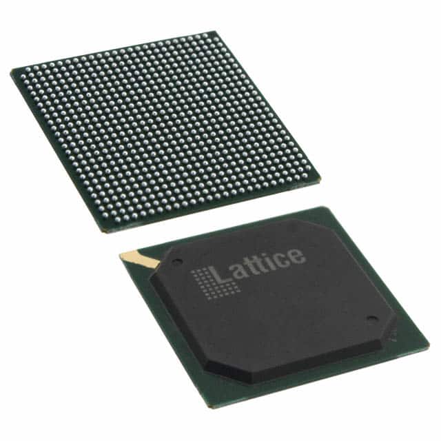
LFE2M50E-5F672C
Product Overview
Category
The LFE2M50E-5F672C belongs to the category of Field Programmable Gate Arrays (FPGAs).
Use
FPGAs are integrated circuits that can be programmed and reprogrammed to perform various digital functions. The LFE2M50E-5F672C is specifically designed for applications requiring high-performance and low-power consumption.
Characteristics
- High-performance FPGA with low power consumption
- Programmable and reprogrammable functionality
- Suitable for a wide range of applications
- Compact package size
Package
The LFE2M50E-5F672C comes in a compact package, ensuring easy integration into electronic systems. It is available in a surface-mount package.
Essence
The essence of the LFE2M50E-5F672C lies in its ability to provide flexible and customizable digital logic functions. It allows designers to implement complex digital systems without the need for custom-designed integrated circuits.
Packaging/Quantity
The LFE2M50E-5F672C is typically packaged in reels or trays, depending on the manufacturer's specifications. The quantity per package may vary, but it is commonly available in quantities suitable for both prototyping and production purposes.
Specifications
- FPGA Family: Lattice ECP2M
- Logic Elements: 50,000
- Speed Grade: -5
- Package Type: FBGA
- Package Size: 672-ball
- Operating Voltage: 1.2V
- I/O Standards: LVCMOS, LVTTL, SSTL, HSTL, LVDS, RSDS, Mini-LVDS, etc.
- Maximum Operating Frequency: Up to 400 MHz
- Embedded Memory: Up to 4.8 Mbits
- DSP Blocks: Up to 96
- PLLs: Up to 4
Detailed Pin Configuration
The LFE2M50E-5F672C has a total of 672 pins, each serving a specific purpose in the FPGA's functionality. The pin configuration varies depending on the specific application requirements and design considerations. For detailed pin assignments and configurations, please refer to the manufacturer's datasheet.
Functional Features
High-performance Computing: The LFE2M50E-5F672C offers efficient processing capabilities, making it suitable for applications requiring complex computations and data manipulation.
Flexible I/O Interfaces: With support for various I/O standards, the FPGA enables seamless integration with different electronic components and systems.
Reconfigurability: The ability to reprogram the FPGA allows for easy updates and modifications to the digital logic, providing flexibility during the development and deployment stages.
Low Power Consumption: The LFE2M50E-5F672C is designed to minimize power consumption while maintaining high performance, making it ideal for battery-powered devices or energy-efficient applications.
Advantages and Disadvantages
Advantages
- Versatility: The FPGA's programmable nature allows for a wide range of applications, making it suitable for diverse industries.
- Time-to-Market: FPGAs enable rapid prototyping and development cycles, reducing time-to-market for new products.
- Cost-Effective: By eliminating the need for custom-designed integrated circuits, FPGAs can significantly reduce production costs.
Disadvantages
- Complexity: Designing and programming FPGAs require specialized knowledge and expertise, which may pose challenges for inexperienced users.
- Resource Limitations: The available logic elements, memory, and other resources within an FPGA are finite, which may restrict the complexity of designs that can be implemented.
Working Principles
FPGAs consist of an array of configurable logic blocks (CLBs) interconnected through programmable routing resources. The LFE2M50E-5F672C utilizes look-up tables (LUTs) within the CLBs to implement digital logic functions. These functions are defined by the user through a hardware description language (HDL) and synthesized into a configuration bitstream that is loaded onto the FPGA.
During operation, the FPGA's internal interconnects route signals between different CLBs, allowing for the execution of complex digital operations. The reprogrammable nature of FPGAs enables designers to modify the functionality of the device without requiring physical changes to the circuitry.
Detailed Application Field Plans
The LFE2M50E-5F672C finds applications in various fields, including:
- Communications: Used in wireless base stations, routers, and network switches to handle high-speed data processing and protocol conversions.
- Industrial Automation: Employed in control systems, robotics, and machine vision applications for real-time data processing and control.
- Automotive: Integrated into advanced driver-assistance systems (ADAS), infotainment systems, and engine control units (EC
Lista 10 Vanliga frågor och svar relaterade till tillämpningen av LFE2M50E-5F672C i tekniska lösningar
Sure! Here are 10 common questions and answers related to the application of LFE2M50E-5F672C in technical solutions:
Q: What is the LFE2M50E-5F672C? A: The LFE2M50E-5F672C is a specific model of FPGA (Field-Programmable Gate Array) manufactured by Lattice Semiconductor.
Q: What are the key features of the LFE2M50E-5F672C? A: Some key features of this FPGA include 50,000 logic elements, 672 pins, low power consumption, and high-speed performance.
Q: What are the typical applications of the LFE2M50E-5F672C? A: This FPGA is commonly used in various technical solutions such as industrial automation, telecommunications, automotive electronics, and medical devices.
Q: How can I program the LFE2M50E-5F672C? A: You can program this FPGA using hardware description languages (HDLs) like VHDL or Verilog, along with specialized software tools provided by Lattice Semiconductor.
Q: Can I reprogram the LFE2M50E-5F672C after it has been programmed once? A: Yes, FPGAs are designed to be reprogrammable, allowing you to modify the functionality of the device even after it has been initially programmed.
Q: What are the advantages of using the LFE2M50E-5F672C in technical solutions? A: Some advantages include its flexibility, ability to implement complex digital designs, fast time-to-market, and cost-effectiveness compared to custom ASICs.
Q: Are there any limitations or considerations when using the LFE2M50E-5F672C? A: Some considerations include power consumption, heat dissipation, and the need for proper signal integrity and timing analysis during design.
Q: Can I interface the LFE2M50E-5F672C with other electronic components or devices? A: Yes, this FPGA supports various communication protocols such as SPI, I2C, UART, and can be interfaced with other components like sensors, displays, and microcontrollers.
Q: Are there any development boards or evaluation kits available for the LFE2M50E-5F672C? A: Yes, Lattice Semiconductor provides development boards and evaluation kits specifically designed for this FPGA, which can help in prototyping and testing.
Q: Where can I find technical documentation and support for the LFE2M50E-5F672C? A: You can find technical documentation, datasheets, application notes, and support resources on the official website of Lattice Semiconductor or by contacting their customer support team.
Please note that the specific details and answers may vary depending on the manufacturer's documentation and guidelines.