

LFE2M50E-6F900I
Product Overview
Category
The LFE2M50E-6F900I belongs to the category of Field Programmable Gate Arrays (FPGAs).
Use
FPGAs are integrated circuits that can be programmed and reprogrammed to perform various digital functions. The LFE2M50E-6F900I is specifically designed for applications requiring high-performance and low-power consumption.
Characteristics
- High-performance FPGA with low power consumption
- Programmable and reprogrammable
- Versatile and flexible in design implementation
Package
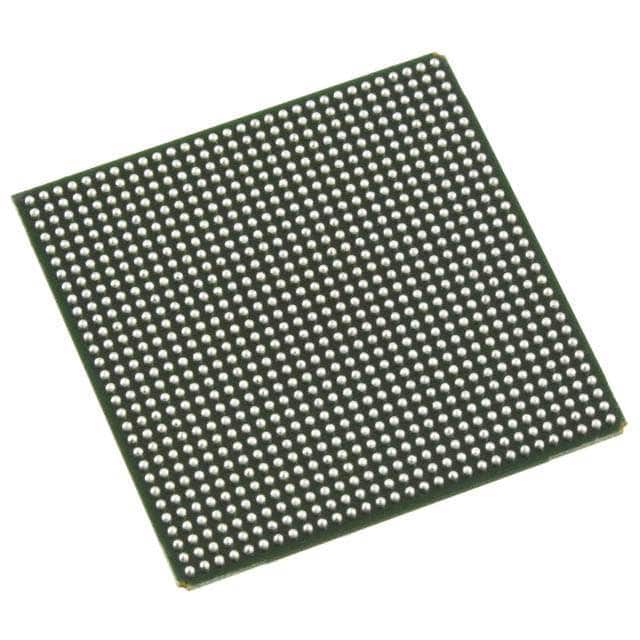
The LFE2M50E-6F900I comes in a compact package suitable for easy integration onto circuit boards.
Essence
The essence of the LFE2M50E-6F900I lies in its ability to provide a customizable and efficient solution for digital circuit design.
Packaging/Quantity
The LFE2M50E-6F900I is typically packaged individually and is available in various quantities depending on the specific requirements of the user.
Specifications
- Model: LFE2M50E-6F900I
- Logic Elements: 50,000
- Speed Grade: 6
- Operating Voltage: 1.2V
- Package Type: FineLine BGA
- I/O Pins: 900
- Memory Blocks: 2,048
- Maximum Frequency: 900 MHz
- Power Consumption: Low
Detailed Pin Configuration
The LFE2M50E-6F900I has a comprehensive pin configuration that enables connectivity and functionality within a digital circuit. The detailed pin configuration can be found in the product datasheet provided by the manufacturer.
Functional Features
- High-performance computing capabilities
- Low power consumption for energy-efficient operation
- Configurable logic elements for versatile design implementation
- Ample memory blocks for data storage and processing
- Extensive I/O pins for connectivity with external devices
Advantages and Disadvantages
Advantages
- High-performance capabilities suitable for demanding applications
- Low power consumption for energy efficiency
- Versatile and flexible design implementation
- Ample memory capacity for data storage and processing
Disadvantages
- Complexity in programming and configuration
- Higher cost compared to other digital circuit solutions
- Limited availability of alternative models
Working Principles
The LFE2M50E-6F900I operates based on the principles of field programmable gate arrays. It consists of configurable logic elements, memory blocks, and input/output pins that can be programmed to perform specific digital functions. The FPGA is configured using a hardware description language (HDL) or a graphical user interface (GUI), allowing users to define the desired functionality of the circuit.
Detailed Application Field Plans
The LFE2M50E-6F900I finds application in various fields, including: 1. Telecommunications: Used in network infrastructure equipment for high-speed data processing. 2. Aerospace and Defense: Employed in radar systems, avionics, and secure communication systems. 3. Industrial Automation: Utilized in control systems and robotics for real-time data processing and control. 4. Medical Devices: Integrated into medical imaging systems and diagnostic equipment for high-performance computing. 5. Automotive: Applied in advanced driver-assistance systems (ADAS) and infotainment systems for enhanced functionality.
Detailed and Complete Alternative Models
While the LFE2M50E-6F900I offers high-performance and versatility, there are alternative FPGA models available in the market. Some notable alternatives include: 1. Xilinx Virtex UltraScale+: Offers advanced features and scalability for complex designs. 2. Intel Stratix 10: Provides high-performance computing capabilities and extensive I/O options. 3. Microsemi SmartFusion2: Combines FPGA capabilities with microcontroller functionality for embedded systems.
These alternative models offer different features and specifications, allowing users to choose the most suitable FPGA for their specific application requirements.
In conclusion, the LFE2M50E-6F900I is a high-performance FPGA that offers versatility, low power consumption, and ample memory capacity. It finds applications in various fields, including telecommunications, aerospace, industrial automation, medical devices, and automotive. While it has advantages such as high performance and flexibility, it also has disadvantages like complexity in programming and higher cost. Users can consider alternative models based on their specific needs and requirements.
Lista 10 Vanliga frågor och svar relaterade till tillämpningen av LFE2M50E-6F900I i tekniska lösningar
Sure! Here are 10 common questions and answers related to the application of LFE2M50E-6F900I in technical solutions:
Q: What is the LFE2M50E-6F900I? A: The LFE2M50E-6F900I is a specific model of Field-Programmable Gate Array (FPGA) manufactured by Lattice Semiconductor.
Q: What are the key features of the LFE2M50E-6F900I? A: The key features of this FPGA include 50,000 logic elements, 900 MHz maximum operating frequency, and support for various I/O standards.
Q: What are some typical applications of the LFE2M50E-6F900I? A: This FPGA can be used in a wide range of applications such as industrial automation, telecommunications, automotive electronics, and medical devices.
Q: How can I program the LFE2M50E-6F900I? A: The LFE2M50E-6F900I can be programmed using the Lattice Diamond design software or other compatible programming tools.
Q: What are the power requirements for the LFE2M50E-6F900I? A: The power supply voltage for this FPGA is typically 1.2V, but it also requires additional voltages for I/O banks and configuration.
Q: Can I interface the LFE2M50E-6F900I with other components or microcontrollers? A: Yes, the LFE2M50E-6F900I supports various communication interfaces like SPI, I2C, UART, and GPIOs, allowing easy integration with other components.
Q: Is the LFE2M50E-6F900I suitable for high-speed applications? A: Yes, with a maximum operating frequency of 900 MHz, this FPGA is well-suited for high-speed applications that require fast data processing.
Q: Can I reprogram the LFE2M50E-6F900I multiple times? A: Yes, this FPGA supports in-system programming, allowing you to reprogram it multiple times during development or in the field.
Q: Are there any development boards available for the LFE2M50E-6F900I? A: Yes, Lattice Semiconductor provides development boards specifically designed for the LFE2M50E-6F900I, which can aid in prototyping and evaluation.
Q: Where can I find technical documentation and support for the LFE2M50E-6F900I? A: You can find technical documentation, datasheets, application notes, and support resources on the official website of Lattice Semiconductor or by contacting their customer support team.
Please note that the answers provided here are general and may vary depending on specific requirements and use cases.