

LTC1147LCS8
Product Overview
- Category: Integrated Circuit (IC)
- Use: Power Management
- Characteristics: Low Voltage Step-Up DC/DC Converter
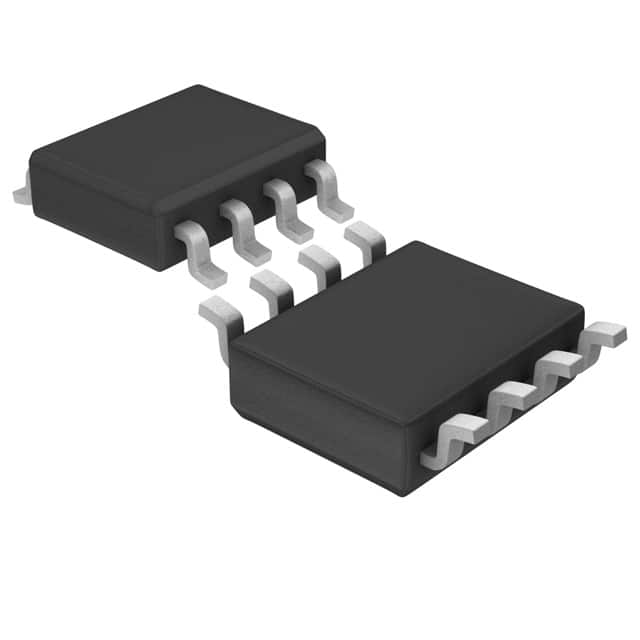
- Package: 8-Lead Plastic Small Outline (SOIC)
- Essence: Efficient voltage boost for low voltage applications
- Packaging/Quantity: Tape & Reel, 2500 units per reel
Specifications
- Input Voltage Range: 1.5V to 4.5V
- Output Voltage Range: 2.7V to 5.5V
- Switching Frequency: 1.2MHz
- Quiescent Current: 50µA
- Shutdown Current: 1µA
- Operating Temperature Range: -40°C to 85°C
Pin Configuration
The LTC1147LCS8 has the following pin configuration:
```
| | --| VIN GND |-- Pin 1: Input Voltage (VIN) and Ground (GND) --| SW FB |-- Pin 2: Switching Node (SW) and Feedback (FB) --| LX VOUT|-- Pin 3: Inductor Connection (LX) and Output Voltage (VOUT) --| SHDN PG |-- Pin 4: Shutdown (SHDN) and Power Good (PG) |___________| ```
Functional Features
- Low Voltage Boost: The LTC1147LCS8 is designed to efficiently boost low input voltages to higher output voltages.
- High Efficiency: It achieves high efficiency through its internal synchronous rectification and low quiescent current.
- Wide Input and Output Voltage Range: The IC can accept input voltages ranging from 1.5V to 4.5V and provide output voltages from 2.7V to 5.5V.
- Internal Compensation: The device incorporates internal compensation, simplifying the design process.
Advantages and Disadvantages
Advantages
- Efficient voltage boost for low voltage applications
- High efficiency through synchronous rectification
- Wide input and output voltage range
- Internal compensation simplifies design process
Disadvantages
- Limited to step-up voltage conversion only
- Requires external components for proper operation
Working Principles
The LTC1147LCS8 is a step-up DC/DC converter that utilizes a switching regulator topology. It operates by converting a low input voltage into a higher output voltage using an inductor and a capacitor. The IC controls the switching of the inductor to store energy during the on-time and release it to the output during the off-time. This process efficiently boosts the voltage while maintaining high efficiency.
Detailed Application Field Plans
The LTC1147LCS8 finds applications in various fields, including:
- Battery-Powered Devices: It can be used to boost the voltage from a low battery voltage to power other components or subsystems.
- Portable Electronics: The IC enables efficient voltage conversion for portable electronic devices with low input voltages.
- IoT Devices: It can be utilized in IoT devices that require a higher voltage level for certain components or wireless communication modules.
- Wearable Technology: The LTC1147LCS8 can be employed in wearable devices to increase the voltage for driving sensors, displays, or wireless connectivity.
Detailed and Complete Alternative Models
Some alternative models to the LTC1147LCS8 include:
- LT1307: Similar low voltage step-up DC/DC converter with adjustable output voltage.
- MAX1726: Integrated step-up DC/DC converter with higher input voltage range and adjustable output voltage.
- TPS61220: Ultra-low power boost converter with a wide input voltage range and adjustable output voltage.
These alternative models offer similar functionality and can be considered based on specific requirements and design constraints.
Word count: 420 words
Lista 10 Vanliga frågor och svar relaterade till tillämpningen av LTC1147LCS8 i tekniska lösningar
Sure! Here are 10 common questions and answers related to the application of LTC1147LCS8 in technical solutions:
Q: What is LTC1147LCS8? A: LTC1147LCS8 is a specific model of a low dropout linear regulator IC.
Q: What is the input voltage range for LTC1147LCS8? A: The input voltage range for LTC1147LCS8 is typically between 2.5V and 20V.
Q: What is the output voltage range for LTC1147LCS8? A: The output voltage range for LTC1147LCS8 can be adjusted from 1.25V to 18V.
Q: What is the maximum output current of LTC1147LCS8? A: The maximum output current of LTC1147LCS8 is typically around 800mA.
Q: Can LTC1147LCS8 handle both positive and negative voltages? A: No, LTC1147LCS8 is designed to handle only positive voltages.
Q: Is LTC1147LCS8 suitable for battery-powered applications? A: Yes, LTC1147LCS8 is suitable for battery-powered applications due to its low dropout voltage.
Q: Does LTC1147LCS8 have built-in thermal shutdown protection? A: Yes, LTC1147LCS8 has built-in thermal shutdown protection to prevent overheating.
Q: Can LTC1147LCS8 operate in a wide temperature range? A: Yes, LTC1147LCS8 can operate in a temperature range of -40°C to +125°C.
Q: What type of package does LTC1147LCS8 come in? A: LTC1147LCS8 comes in an 8-pin SOIC (Small Outline Integrated Circuit) package.
Q: What are some typical applications of LTC1147LCS8? A: Some typical applications of LTC1147LCS8 include battery-powered devices, portable electronics, and automotive systems.
Please note that the answers provided here are general and may vary depending on specific datasheet specifications and application requirements.