

LTC1655LCS8#TRPBF
Product Overview
Category
The LTC1655LCS8#TRPBF belongs to the category of integrated circuits (ICs).
Use
This product is commonly used in electronic devices for digital-to-analog conversion (DAC) applications.
Characteristics
- High precision: The LTC1655LCS8#TRPBF offers exceptional accuracy in converting digital signals to analog outputs.
- Low power consumption: This IC is designed to operate efficiently with minimal power requirements.
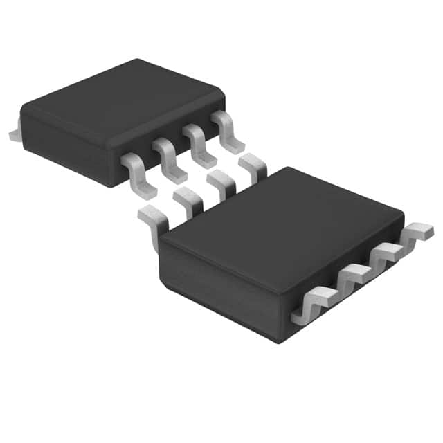
- Small package size: The LTC1655LCS8#TRPBF comes in a compact 8-lead plastic small outline (SOIC) package, making it suitable for space-constrained applications.
- Wide operating voltage range: It can operate within a wide voltage range, providing flexibility in various electronic systems.
- Fast settling time: This IC ensures rapid and accurate conversion of digital signals to analog outputs.
Package and Quantity
The LTC1655LCS8#TRPBF is available in an 8-lead SOIC package. It is typically sold in reels or tubes containing a specific quantity, such as 2500 units per reel.
Specifications
- Resolution: The LTC1655LCS8#TRPBF has a resolution of 16 bits, allowing for precise analog output generation.
- Supply Voltage Range: It can operate within a supply voltage range of 2.7V to 5.5V.
- Output Voltage Range: The output voltage range of this IC is programmable and can be adjusted according to the application requirements.
- Operating Temperature Range: The LTC1655LCS8#TRPBF can function reliably within a temperature range of -40°C to +85°C.
- Digital Interface: It utilizes a standard serial interface (SPI) for communication with microcontrollers or other digital devices.
Pin Configuration
The LTC1655LCS8#TRPBF has the following pin configuration:
- VDD: Power supply voltage input
- CS: Chip select input for SPI communication
- SCLK: Serial clock input for SPI communication
- SDI: Serial data input for SPI communication
- GND: Ground reference
- AGND: Analog ground reference
- OUT: Analog output voltage
- REF: Reference voltage input
Functional Features
- Digital-to-Analog Conversion: The LTC1655LCS8#TRPBF performs high-precision conversion of digital signals to analog outputs.
- Programmable Output Voltage: The output voltage can be programmed to meet specific application requirements.
- Fast Settling Time: This IC ensures rapid settling time, enabling quick response in dynamic applications.
- Low Power Consumption: The LTC1655LCS8#TRPBF is designed to operate efficiently with minimal power consumption.
- SPI Interface: It utilizes a standard serial interface (SPI) for easy integration with microcontrollers and other digital devices.
Advantages and Disadvantages
Advantages
- High precision and accuracy in digital-to-analog conversion.
- Compact package size suitable for space-constrained applications.
- Wide operating voltage range provides flexibility in various electronic systems.
- Fast settling time ensures quick response in dynamic applications.
Disadvantages
- Limited resolution compared to higher-end DACs.
- Requires external components for proper operation.
Working Principles
The LTC1655LCS8#TRPBF operates based on the principle of converting digital signals into corresponding analog voltages. It utilizes an internal digital-to-analog converter (DAC) to convert the digital input into an analog output voltage. The digital input is received through the SPI interface, and the DAC generates the corresponding analog voltage based on the input value. This analog voltage can then be used as a control signal or reference voltage in various electronic systems.
Application Field Plans
The LTC1655LCS8#TRPBF finds applications in various fields, including:
- Industrial Automation: It can be used in industrial control systems to generate precise analog control signals for motor speed control, temperature regulation, and other automation processes.
- Audio Equipment: This IC is suitable for audio devices that require accurate digital-to-analog conversion, such as digital audio players, audio mixers, and amplifiers.
- Test and Measurement Instruments: The LTC1655LCS8#TRPBF can be integrated into test and measurement equipment to provide high-precision analog output signals for calibration and testing purposes.
- Communication Systems: It can be utilized in communication systems for generating analog reference voltages or control signals required for signal processing and modulation.
Alternative Models
Here are some alternative models that offer similar functionality:
- MAX5216: 16-bit DAC with SPI interface and low power consumption.
- AD5667: 16-bit DAC with programmable output voltage range and fast settling time.
- MCP4922: 12-bit
Lista 10 Vanliga frågor och svar relaterade till tillämpningen av LTC1655LCS8#TRPBF i tekniska lösningar
Sure! Here are 10 common questions and answers related to the application of LTC1655LCS8#TRPBF:
Q: What is LTC1655LCS8#TRPBF? A: LTC1655LCS8#TRPBF is a specific model number for a digital-to-analog converter (DAC) chip manufactured by Linear Technology (now part of Analog Devices).
Q: What is the purpose of LTC1655LCS8#TRPBF? A: The LTC1655LCS8#TRPBF DAC is used to convert digital signals into analog voltages, making it suitable for various applications such as instrumentation, control systems, and communication devices.
Q: What is the resolution of LTC1655LCS8#TRPBF? A: The LTC1655LCS8#TRPBF has a resolution of 16 bits, meaning it can provide 65,536 different output voltage levels.
Q: What is the operating voltage range of LTC1655LCS8#TRPBF? A: The LTC1655LCS8#TRPBF operates with a single supply voltage ranging from 2.7V to 5.5V.
Q: How many channels does LTC1655LCS8#TRPBF have? A: The LTC1655LCS8#TRPBF is a single-channel DAC, meaning it can generate one analog output voltage at a time.
Q: What is the maximum output voltage range of LTC1655LCS8#TRPBF? A: The LTC1655LCS8#TRPBF can generate an output voltage range from 0V to Vref, where Vref is the reference voltage supplied to the chip.
Q: How is LTC1655LCS8#TRPBF controlled? A: The LTC1655LCS8#TRPBF can be controlled using a serial interface, such as SPI (Serial Peripheral Interface) or I2C (Inter-Integrated Circuit).
Q: Can LTC1655LCS8#TRPBF operate in both unipolar and bipolar modes? A: Yes, the LTC1655LCS8#TRPBF can operate in both unipolar mode (0V to Vref) and bipolar mode (-Vref/2 to +Vref/2), depending on the application requirements.
Q: Does LTC1655LCS8#TRPBF have any built-in features for accuracy and precision? A: Yes, the LTC1655LCS8#TRPBF includes an internal reference voltage and a precision voltage reference input pin for improved accuracy and stability.
Q: What is the package type of LTC1655LCS8#TRPBF? A: LTC1655LCS8#TRPBF is available in an 8-pin SOIC (Small Outline Integrated Circuit) package, which is commonly used in surface-mount applications.
Please note that the answers provided here are general and may vary depending on the specific datasheet and application notes provided by the manufacturer.