

AT49F512-70PI
Product Overview
Category
AT49F512-70PI belongs to the category of non-volatile memory devices.
Use
It is primarily used for storing and retrieving digital information in electronic systems.
Characteristics
- Non-volatile: Retains data even when power is turned off.
- High storage capacity: 512 kilobits (64 kilobytes).
- Fast access time: Operates at a speed of 70 nanoseconds.
- Low power consumption: Designed to minimize energy usage.
- Durable: Can withstand harsh environmental conditions.
- Easy integration: Compatible with various electronic systems.
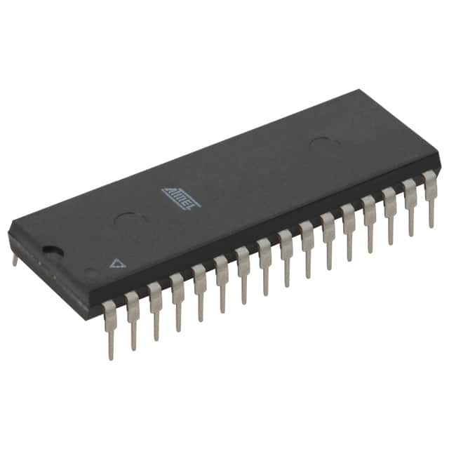
Package
AT49F512-70PI is available in a plastic integrated circuit package.
Essence
The essence of AT49F512-70PI lies in its ability to provide reliable and high-capacity non-volatile memory storage for electronic devices.
Packaging/Quantity
This product is typically packaged in reels or tubes, with each containing a specific quantity of AT49F512-70PI chips.
Specifications
- Memory Type: Flash EEPROM
- Memory Size: 512 kilobits (64 kilobytes)
- Access Time: 70 nanoseconds
- Supply Voltage: 5V
- Operating Temperature Range: -40°C to +85°C
- Package Type: Plastic Integrated Circuit
Detailed Pin Configuration
- VCC: Power supply voltage
- A0-A16: Address inputs
- CE: Chip enable
- OE: Output enable
- WE: Write enable
- I/O0-I/O7: Data input/output
- RY/BY: Ready/Busy output
- RESET: Reset input
Functional Features
- High-speed read and write operations
- Sector erase capability
- Byte programming capability
- Automatic sleep mode to conserve power
- Hardware and software data protection mechanisms
- Easy integration with various microcontrollers and systems
Advantages
- Non-volatile memory ensures data retention even during power loss.
- High storage capacity allows for storing large amounts of information.
- Fast access time enables quick retrieval of data.
- Low power consumption helps in energy-efficient designs.
- Durable construction ensures reliability in challenging environments.
- Compatibility with different electronic systems enhances versatility.
Disadvantages
- Limited storage capacity compared to other memory technologies.
- Relatively slower write speeds compared to volatile memory.
- Higher cost per bit compared to some alternative memory solutions.
Working Principles
AT49F512-70PI utilizes flash EEPROM technology, which combines the advantages of both EPROM and EEPROM. It stores data using floating gate transistors that can retain charge even when power is removed. The memory cells are organized into sectors, allowing for efficient erasing and programming operations. The device operates by applying appropriate voltage levels to the control pins, enabling read, write, erase, and other operations.
Detailed Application Field Plans
AT49F512-70PI finds applications in various electronic systems, including but not limited to: - Embedded systems - Consumer electronics - Automotive electronics - Industrial control systems - Communication devices - Medical equipment
Detailed and Complete Alternative Models
- AT49BV512-70VI: Similar specifications with extended voltage range.
- AT45DB641E-SHN-T: Serial interface flash memory with higher storage capacity.
- W25Q64JVZPIQ: Quad SPI flash memory with faster transfer rates.
- M25P16-VMN6TPB: Serial NOR flash memory with smaller package size.
These alternative models offer different features and capabilities, allowing users to choose the most suitable option based on their specific requirements.
Word Count: 550 words
Lista 10 Vanliga frågor och svar relaterade till tillämpningen av AT49F512-70PI i tekniska lösningar
Sure! Here are 10 common questions and answers related to the application of AT49F512-70PI in technical solutions:
Q: What is the AT49F512-70PI? A: The AT49F512-70PI is a 512K (64K x 8) CMOS flash memory chip manufactured by Atmel.
Q: What is the operating voltage range for the AT49F512-70PI? A: The AT49F512-70PI operates within a voltage range of 4.5V to 5.5V.
Q: What is the maximum clock frequency supported by the AT49F512-70PI? A: The AT49F512-70PI supports a maximum clock frequency of 70 MHz.
Q: Can the AT49F512-70PI be used as a boot device in embedded systems? A: Yes, the AT49F512-70PI can be used as a boot device due to its fast access times and non-volatile storage capabilities.
Q: How many write/erase cycles can the AT49F512-70PI endure? A: The AT49F512-70PI can endure a minimum of 100,000 write/erase cycles.
Q: What is the typical access time for reading data from the AT49F512-70PI? A: The typical access time for reading data from the AT49F512-70PI is 70 ns.
Q: Can the AT49F512-70PI be directly interfaced with microcontrollers? A: Yes, the AT49F512-70PI can be directly interfaced with microcontrollers using standard parallel interface protocols.
Q: Does the AT49F512-70PI support in-system programming (ISP)? A: No, the AT49F512-70PI does not support in-system programming. It requires a separate programmer device.
Q: What is the temperature range within which the AT49F512-70PI can operate? A: The AT49F512-70PI can operate within a temperature range of -40°C to +85°C.
Q: Are there any specific precautions to be taken while handling the AT49F512-70PI? A: Yes, it is important to handle the AT49F512-70PI with proper electrostatic discharge (ESD) precautions to avoid damage to the chip.
Please note that these answers are general and may vary depending on the specific application and requirements.