

Se specifikationer för produktinformation.
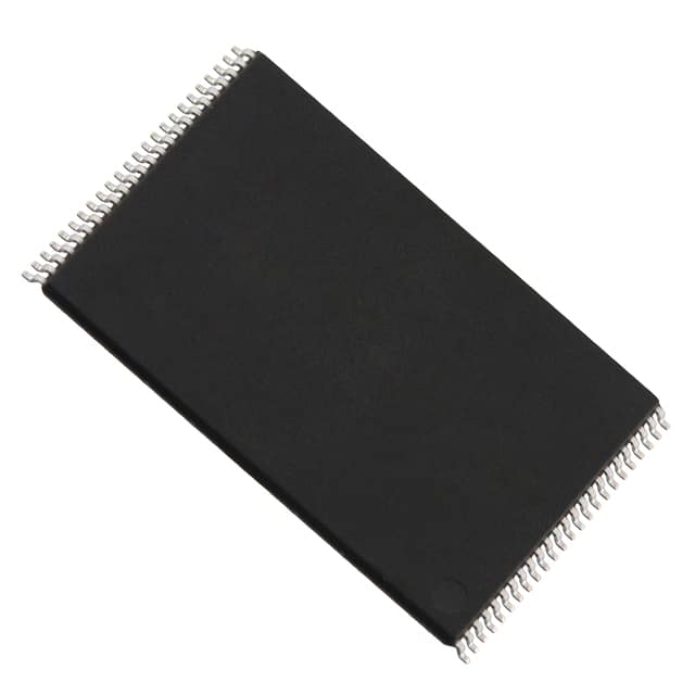
NAND08GW3C2BN6E
Product Overview
- Category: NAND Flash Memory
- Use: Data storage in electronic devices
- Characteristics:
- High capacity
- Fast read and write speeds
- Low power consumption
- Compact size
- Package: BGA (Ball Grid Array)
- Essence: Non-volatile memory for storing digital data
- Packaging/Quantity: Individually packaged, quantity varies based on manufacturer
Specifications
- Capacity: 8GB
- Interface: Serial Peripheral Interface (SPI)
- Voltage Supply: 2.7V - 3.6V
- Operating Temperature: -40°C to +85°C
- Data Retention: Up to 10 years
- Endurance: Up to 100,000 program/erase cycles
Detailed Pin Configuration
The NAND08GW3C2BN6E has a standard pin configuration as follows:
- VCC: Power supply voltage
- GND: Ground
- /CE: Chip enable
- /WP: Write protect
- SIO0: Serial data input/output
- SIO1: Serial data input/output
- SIO2: Serial data input/output
- SIO3: Serial data input/output
- CLE: Command latch enable
- ALE: Address latch enable
- /RE: Read enable
- /WE: Write enable
- R/B: Ready/busy status
- NC: No connection
- NC: No connection
- NC: No connection
Functional Features
- High-speed data transfer
- Error correction capability
- Block management for efficient data organization
- Wear-leveling algorithm for extended lifespan
- Bad block management for improved reliability
- Power-saving features for low energy consumption
Advantages and Disadvantages
Advantages: - Large storage capacity - Fast read and write speeds - Compact size for space-constrained devices - Low power consumption - Reliable data retention
Disadvantages: - Limited endurance compared to other memory technologies - Higher cost per gigabyte compared to traditional hard drives
Working Principles
The NAND08GW3C2BN6E utilizes NAND flash memory technology, which stores data in a series of memory cells organized in a grid-like structure. It employs a floating gate transistor design, where the presence or absence of an electric charge determines the stored data. When reading data, the controller applies voltages to specific cells and measures the resulting electrical current to determine the stored value. During writing, the controller applies higher voltages to program the desired data into the cells.
Detailed Application Field Plans
The NAND08GW3C2BN6E is widely used in various electronic devices that require non-volatile data storage, including but not limited to: - Smartphones and tablets - Solid-state drives (SSDs) - Digital cameras - Portable media players - Automotive infotainment systems - Industrial control systems
Alternative Models
- NAND16GW3C2BN6E: 16GB capacity, same specifications as NAND08GW3C2BN6E
- NAND32GW3C2BN6E: 32GB capacity, same specifications as NAND08GW3C2BN6E
- NAND64GW3C2BN6E: 64GB capacity, same specifications as NAND08GW3C2BN6E
These alternative models offer increased storage capacity while maintaining compatibility with the NAND08GW3C2BN6E in terms of pin configuration and functionality.
In conclusion, the NAND08GW3C2BN6E is a high-capacity NAND flash memory device designed for data storage in various electronic devices. With its fast read and write speeds, low power consumption, and compact size, it offers a reliable solution for storing digital data. Its functional features, such as error correction capability and wear-leveling algorithm, further enhance its performance and lifespan. While it has limitations in terms of endurance and cost, the NAND08GW3C2BN6E remains a popular choice in the industry due to its overall advantages and compatibility with alternative models.
Lista 10 Vanliga frågor och svar relaterade till tillämpningen av NAND08GW3C2BN6E i tekniska lösningar
Sure! Here are 10 common questions and answers related to the application of NAND08GW3C2BN6E in technical solutions:
Q: What is NAND08GW3C2BN6E? A: NAND08GW3C2BN6E is a specific model of NAND flash memory chip manufactured by a particular company.
Q: What is the storage capacity of NAND08GW3C2BN6E? A: NAND08GW3C2BN6E has a storage capacity of 8 gigabytes (GB).
Q: What is the interface used by NAND08GW3C2BN6E? A: NAND08GW3C2BN6E uses a standard NAND flash interface for data transfer.
Q: Can NAND08GW3C2BN6E be used in consumer electronics devices? A: Yes, NAND08GW3C2BN6E is commonly used in various consumer electronics devices like smartphones, tablets, and portable media players.
Q: Is NAND08GW3C2BN6E suitable for industrial applications? A: Yes, NAND08GW3C2BN6E is designed to meet the requirements of industrial applications, including automotive, medical, and aerospace industries.
Q: What is the operating voltage range of NAND08GW3C2BN6E? A: NAND08GW3C2BN6E operates within a voltage range of typically 2.7V to 3.6V.
Q: Does NAND08GW3C2BN6E support wear-leveling algorithms? A: Yes, NAND08GW3C2BN6E supports wear-leveling algorithms to distribute write operations evenly across memory blocks, extending the lifespan of the chip.
Q: Can NAND08GW3C2BN6E be used as a boot device? A: Yes, NAND08GW3C2BN6E can be used as a boot device in embedded systems and other applications that require fast startup times.
Q: What is the maximum data transfer rate of NAND08GW3C2BN6E? A: NAND08GW3C2BN6E has a maximum data transfer rate of typically 400 megabytes per second (MB/s).
Q: Are there any specific temperature requirements for NAND08GW3C2BN6E? A: NAND08GW3C2BN6E is designed to operate within a wide temperature range, typically from -40°C to +85°C, making it suitable for various environments.
Please note that the answers provided here are general and may vary depending on the specific implementation and datasheet of NAND08GW3C2BN6E.