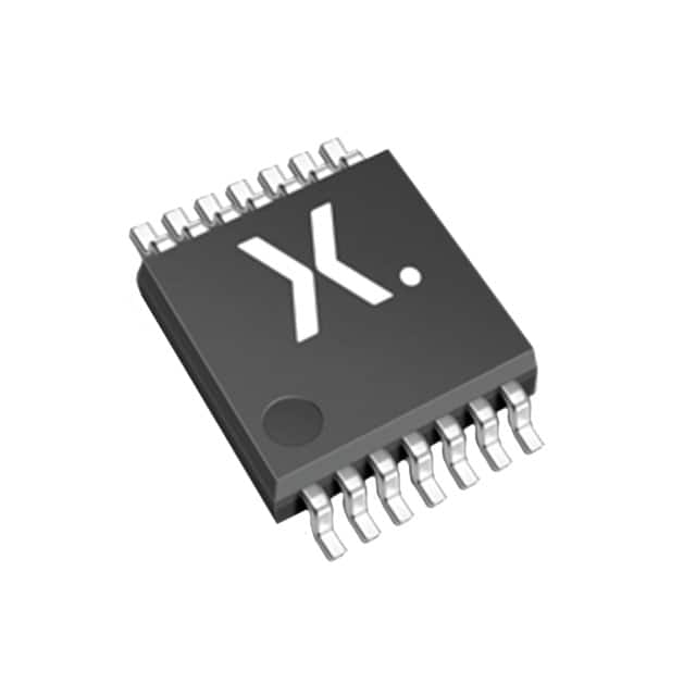
Encyclopedia Entry: 74AHCT02PW,112
Product Overview
Category
The 74AHCT02PW,112 belongs to the category of integrated circuits (ICs).
Use
This product is commonly used in electronic devices for digital logic applications.
Characteristics
- High-speed operation
- Low power consumption
- Wide operating voltage range
- Compatibility with TTL input levels
- Schmitt-trigger action on all inputs
Package
The 74AHCT02PW,112 is available in a small-sized TSSOP-14 package.
Essence
The essence of this product lies in its ability to perform logical operations efficiently and reliably within electronic circuits.
Packaging/Quantity
The 74AHCT02PW,112 is typically packaged in reels or tubes, containing a quantity of 2500 units per reel/tube.
Specifications
- Supply Voltage Range: 2 V to 5.5 V
- Input Voltage Range: -0.5 V to VCC + 0.5 V
- Output Voltage Range: 0 V to VCC
- Operating Temperature Range: -40°C to +125°C
- Propagation Delay Time: 6 ns (max)
- Quiescent Current: 4 μA (typ)
Detailed Pin Configuration
The 74AHCT02PW,112 has a total of 14 pins, numbered as follows:
- Input A1
- Input B1
- Output Y1
- Ground (GND)
- Input A2
- Input B2
- Output Y2
- VCC (Supply Voltage)
- Input A3
- Input B3
- Output Y3
- Input A4
- Input B4
- Output Y4
Functional Features
- The 74AHCT02PW,112 consists of four independent 2-input NOR gates.
- It operates at high speed, making it suitable for applications requiring quick response times.
- The low power consumption of this IC helps in reducing overall energy usage.
- Its wide operating voltage range allows compatibility with various power supply configurations.
- The Schmitt-trigger action on all inputs ensures reliable and noise-immune operation.
Advantages and Disadvantages
Advantages
- High-speed operation enables efficient processing of digital signals.
- Low power consumption contributes to energy efficiency.
- Wide operating voltage range enhances versatility.
- Compatibility with TTL input levels simplifies integration into existing systems.
- Schmitt-trigger action provides robustness against noise.
Disadvantages
- Limited number of gates per package may require multiple ICs for complex circuits.
- Sensitive to electrostatic discharge (ESD), necessitating proper handling precautions.
Working Principles
The 74AHCT02PW,112 functions based on the principles of NOR gate logic. Each gate within the IC accepts two input signals and produces an output signal according to the NOR truth table. The Schmitt-trigger action ensures that the output transitions occur at well-defined voltage levels, even in the presence of noisy input signals.
Detailed Application Field Plans
The 74AHCT02PW,112 finds application in various electronic systems, including but not limited to: - Digital data processing - Communication devices - Microcontrollers - Industrial automation - Automotive electronics
Detailed and Complete Alternative Models
There are several alternative models available in the market that offer similar functionality to the 74AHCT02PW,112. Some notable alternatives include: - 74HC02: This IC is compatible with CMOS logic levels and offers similar performance characteristics. - SN74LS02: A popular TTL-compatible alternative with comparable specifications. - CD4001: A versatile CMOS-based quad NOR gate IC.
These alternative models can be considered based on specific project requirements and availability.
Word count: 505 words
Lista 10 Vanliga frågor och svar relaterade till tillämpningen av 74AHCT02PW,112 i tekniska lösningar
Sure! Here are 10 common questions and answers related to the application of 74AHCT02PW,112 in technical solutions:
Q: What is the 74AHCT02PW,112? A: The 74AHCT02PW,112 is a quad 2-input NOR gate integrated circuit (IC) that operates on a supply voltage range of 4.5V to 5.5V.
Q: What is the purpose of a NOR gate? A: A NOR gate is a logic gate that produces an output signal only when all of its inputs are low (logic 0).
Q: What are some typical applications of the 74AHCT02PW,112? A: The 74AHCT02PW,112 can be used in various applications such as digital systems, computers, communication devices, and control circuits.
Q: How many inputs does the 74AHCT02PW,112 have? A: The 74AHCT02PW,112 has four inputs, allowing you to connect up to four different input signals.
Q: What is the maximum operating frequency of the 74AHCT02PW,112? A: The maximum operating frequency of the 74AHCT02PW,112 is typically around 125 MHz.
Q: What is the output voltage level of the 74AHCT02PW,112? A: The output voltage level of the 74AHCT02PW,112 is compatible with both TTL and CMOS logic levels.
Q: Can the 74AHCT02PW,112 be used in high-speed applications? A: Yes, the 74AHCT02PW,112 is designed for high-speed operation, making it suitable for use in high-speed applications.
Q: What is the power supply voltage range for the 74AHCT02PW,112? A: The 74AHCT02PW,112 operates on a power supply voltage range of 4.5V to 5.5V.
Q: Does the 74AHCT02PW,112 have any built-in protection features? A: Yes, the 74AHCT02PW,112 has built-in ESD (electrostatic discharge) protection to prevent damage from static electricity.
Q: Can I use multiple 74AHCT02PW,112 ICs together in my circuit? A: Yes, you can easily connect multiple 74AHCT02PW,112 ICs together to expand the number of inputs or outputs in your circuit.
Please note that these answers are general and may vary depending on specific datasheet specifications and application requirements.


