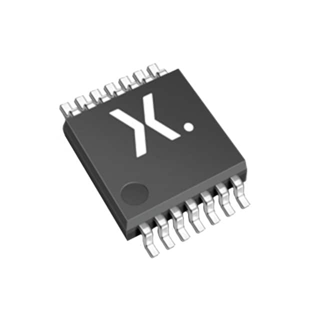
Encyclopedia Entry: 74ALVC14PW,112
Product Information Overview
- Category: Integrated Circuit (IC)
- Use: Logic Gate Inverter
- Characteristics: High-speed, low-power, Schmitt-trigger input, wide operating voltage range
- Package: TSSOP-14
- Essence: Hex Schmitt-trigger inverter
- Packaging/Quantity: Tape and Reel, 2500 units per reel
Specifications
- Supply Voltage Range: 1.2V to 3.6V
- Input Voltage Range: -0.5V to VCC + 0.5V
- Output Voltage Range: 0V to VCC
- Operating Temperature Range: -40°C to +85°C
- Propagation Delay: 3.8ns (typical) at 3.3V supply voltage
- Quiescent Current: 10μA (typical) at 3.3V supply voltage
Detailed Pin Configuration
The 74ALVC14PW,112 IC has a TSSOP-14 package with the following pin configuration:
__    __
   Y1 | 1    14 | VCC
   A1 | 2    13 | Y2
   A2 | 3    12 | Y3
   Y4 | 4    11 | A3
   A4 | 5    10 | Y5
   Y6 | 6     9 | A5
 GND  | 7     8 | Y7
       ‾‾    ‾‾
Functional Features
- Hex Schmitt-trigger inverters for signal conditioning applications
- Wide operating voltage range allows compatibility with various systems
- High-speed operation enables efficient signal processing
- Low-power consumption for energy-efficient designs
- Schmitt-trigger input ensures noise immunity and hysteresis
Advantages and Disadvantages
Advantages: - High-speed operation improves system performance - Low-power consumption extends battery life in portable devices - Wide operating voltage range enhances compatibility - Schmitt-trigger input provides noise immunity and stable output
Disadvantages: - Limited number of inverters (6) in a single package - TSSOP package may require careful handling during assembly
Working Principles
The 74ALVC14PW,112 is a hex Schmitt-trigger inverter IC. It takes an input signal and produces the inverted output signal. The Schmitt-trigger input ensures that the output transitions occur at different voltage levels for rising and falling input signals. This hysteresis property provides noise immunity and stable output even in the presence of input signal fluctuations.
Detailed Application Field Plans
The 74ALVC14PW,112 finds applications in various fields, including:
- Digital Communication Systems: Signal conditioning and level shifting in data transmission circuits.
- Automotive Electronics: Noise filtering and signal amplification in automotive control systems.
- Industrial Automation: Interface circuitry for sensors, actuators, and control modules.
- Consumer Electronics: Logic level conversion and signal buffering in audio/video equipment.
- Computer Hardware: Clock signal generation and synchronization in microprocessors and memory modules.
Detailed and Complete Alternative Models
Some alternative models to the 74ALVC14PW,112 include:
- SN74LVC14A - Hex Schmitt-trigger inverter by Texas Instruments.
- MC74VHC1G14 - Single Schmitt-trigger inverter by ON Semiconductor.
- CD40106B - Hex Schmitt-trigger inverter by Texas Instruments.
- 74HC14 - Hex Schmitt-trigger inverter by NXP Semiconductors.
These alternative models offer similar functionality and can be used as substitutes depending on specific requirements.
Word Count: 410 words
Lista 10 Vanliga frågor och svar relaterade till tillämpningen av 74ALVC14PW,112 i tekniska lösningar
Sure! Here are 10 common questions and answers related to the application of 74ALVC14PW,112:
Q: What is the 74ALVC14PW,112? A: The 74ALVC14PW,112 is a hex inverter with Schmitt-trigger inputs. It is a commonly used integrated circuit (IC) in digital electronics.
Q: What is the purpose of a hex inverter? A: A hex inverter is used to invert the logic level of an input signal. It converts a high-level input to a low-level output and vice versa.
Q: What are Schmitt-trigger inputs? A: Schmitt-trigger inputs are a type of input circuitry that provide hysteresis, allowing for better noise immunity and more stable switching behavior.
Q: What is the voltage supply range for the 74ALVC14PW,112? A: The 74ALVC14PW,112 operates with a voltage supply range of 1.65V to 5.5V.
Q: How many inverters are there in the 74ALVC14PW,112? A: The 74ALVC14PW,112 contains six individual inverters.
Q: What is the maximum output current of the 74ALVC14PW,112? A: The maximum output current per channel is typically around 24mA.
Q: Can the 74ALVC14PW,112 be used in both CMOS and TTL logic systems? A: Yes, the 74ALVC14PW,112 is compatible with both CMOS and TTL logic levels.
Q: What is the propagation delay of the 74ALVC14PW,112? A: The propagation delay is the time it takes for a change in the input to be reflected at the output. For the 74ALVC14PW,112, the typical propagation delay is around 3.5ns.
Q: Can the 74ALVC14PW,112 be used in high-speed applications? A: Yes, the 74ALVC14PW,112 is designed for high-speed operation and can be used in various high-frequency applications.
Q: Are there any specific precautions to consider when using the 74ALVC14PW,112? A: It is important to ensure proper decoupling capacitors are used near the power supply pins of the IC to minimize noise and voltage fluctuations. Additionally, care should be taken to avoid exceeding the maximum ratings specified in the datasheet, such as voltage and temperature limits.
Please note that these answers are general and may vary depending on the specific application and requirements. Always refer to the datasheet and consult with an expert for accurate information.


