

Encyclopedia Entry: 74AUP2G00GN,115
Product Overview
- Category: Integrated Circuit (IC)
- Use: Logic Gate
- Characteristics: High-speed, Low-power consumption
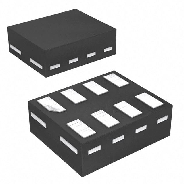
- Package: SOT353 (Thin Small Outline Transistor)
- Essence: Dual 2-input NAND gate
- Packaging/Quantity: Tape and Reel, 3000 pieces per reel
Specifications
- Supply Voltage: 0.8V to 3.6V
- Input Voltage: -0.5V to VCC + 0.5V
- Output Voltage: -0.5V to VCC + 0.5V
- Operating Temperature Range: -40°C to +125°C
- Propagation Delay: 1.9 ns (typical) at 3.3V supply voltage
Detailed Pin Configuration
The 74AUP2G00GN,115 IC has a total of 6 pins: 1. Pin 1: Input A 2. Pin 2: Input B 3. Pin 3: Ground (GND) 4. Pin 4: Output Y 5. Pin 5: Power Supply (VCC) 6. Pin 6: No Connection (NC)
Functional Features
- Dual 2-input NAND gate with Schmitt-trigger inputs
- High-speed operation with low power consumption
- Wide operating voltage range for versatile applications
- Schmitt-trigger inputs provide hysteresis and improve noise immunity
Advantages and Disadvantages
Advantages: - High-speed performance enables efficient data processing - Low-power consumption reduces energy usage - Schmitt-trigger inputs enhance noise immunity and signal integrity
Disadvantages: - Limited number of inputs and outputs restricts complex logic operations - SOT353 package may require specialized handling during assembly
Working Principles
The 74AUP2G00GN,115 is a dual 2-input NAND gate that performs logical AND operation on two input signals. It utilizes Schmitt-trigger inputs, which provide hysteresis and improve noise immunity by ensuring a clean transition between logic levels. The IC operates within a wide voltage range and consumes minimal power while delivering high-speed performance.
Detailed Application Field Plans
The 74AUP2G00GN,115 finds applications in various fields, including: 1. Digital electronics 2. Communication systems 3. Microcontrollers 4. Signal processing 5. Industrial automation
Alternative Models
Other alternative models that can be considered as replacements for the 74AUP2G00GN,115 include: 1. SN74LVC2G00DBVR - Dual 2-input NAND gate with similar characteristics 2. MC74VHC1G00DTT1G - Single 2-input NAND gate with comparable specifications 3. CD4011BE - Quad 2-input NAND gate for more complex logic operations
Note: This encyclopedia entry provides an overview of the 74AUP2G00GN,115 IC, its specifications, pin configuration, functional features, advantages and disadvantages, working principles, application field plans, and alternative models.
Lista 10 Vanliga frågor och svar relaterade till tillämpningen av 74AUP2G00GN,115 i tekniska lösningar
Sure! Here are 10 common questions and answers related to the application of 74AUP2G00GN,115 in technical solutions:
1. What is the 74AUP2G00GN,115? The 74AUP2G00GN,115 is a dual 2-input NAND gate integrated circuit (IC) that operates at low voltage levels.
2. What is the operating voltage range of the 74AUP2G00GN,115? The operating voltage range of the 74AUP2G00GN,115 is typically between 0.8V and 3.6V.
3. What is the maximum output current of the 74AUP2G00GN,115? The maximum output current of the 74AUP2G00GN,115 is around 32mA.
4. Can the 74AUP2G00GN,115 be used in battery-powered applications? Yes, the 74AUP2G00GN,115 can be used in battery-powered applications due to its low power consumption and wide operating voltage range.
5. What is the propagation delay of the 74AUP2G00GN,115? The propagation delay of the 74AUP2G00GN,115 is typically around 2.5ns.
6. Is the 74AUP2G00GN,115 suitable for high-speed applications? Yes, the 74AUP2G00GN,115 is suitable for high-speed applications due to its fast switching speed and low propagation delay.
7. Can the 74AUP2G00GN,115 be used in both digital and analog circuits? No, the 74AUP2G00GN,115 is primarily designed for digital logic applications and may not be suitable for analog circuits.
8. What is the package type of the 74AUP2G00GN,115? The 74AUP2G00GN,115 is available in a small SOT353 (SC-88) package.
9. Can the 74AUP2G00GN,115 be used in automotive applications? Yes, the 74AUP2G00GN,115 is suitable for automotive applications as it meets the necessary automotive standards.
10. Are there any recommended operating conditions for the 74AUP2G00GN,115? Yes, some recommended operating conditions include a supply voltage between 0.8V and 3.6V, an ambient temperature range of -40°C to +125°C, and proper decoupling capacitors for stable operation.
Please note that these answers are general and may vary depending on the specific requirements and datasheet of the 74AUP2G00GN,115.