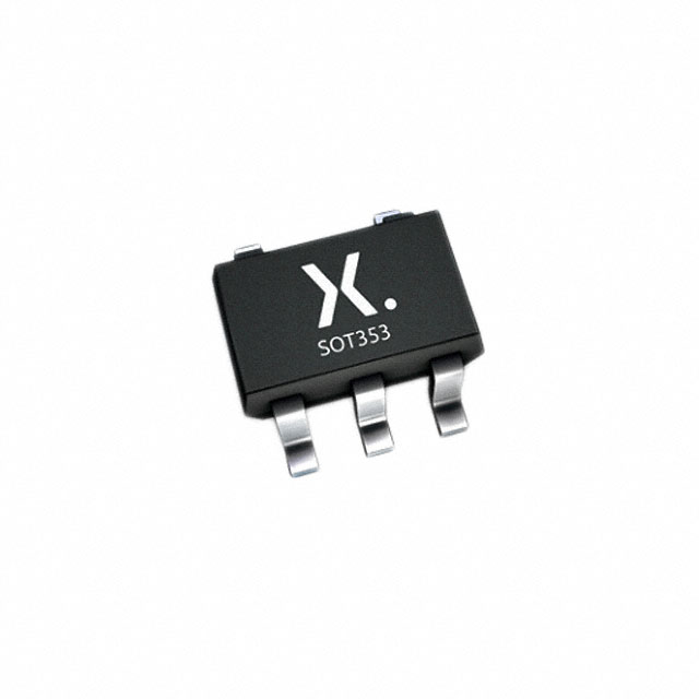
74LVC1G86GW,125
Basic Information Overview
- Category: Integrated Circuit (IC)
- Use: Logic Gate
- Characteristics: Single 2-input XOR gate
- Package: SOT753 (SC-70)
- Essence: High-speed CMOS technology
- Packaging/Quantity: Tape and Reel, 3000 pieces per reel
Specifications
- Supply Voltage Range: 1.65V to 5.5V
- Input Voltage Range: -0.5V to VCC + 0.5V
- Output Voltage Range: GND to VCC
- Operating Temperature Range: -40°C to +125°C
- Propagation Delay: 4.3 ns at 3.3V, 6.8 ns at 1.8V
- Maximum Quiescent Current: 10 µA at 5.5V
Detailed Pin Configuration
The 74LVC1G86GW,125 has a total of 5 pins: 1. A: Input A 2. B: Input B 3. Y: Output 4. GND: Ground 5. VCC: Power Supply
Functional Features
- Low power consumption
- High noise immunity
- Schmitt-trigger input for improved noise rejection
- Balanced propagation delays
- Wide operating voltage range
- Compatible with TTL levels
- ESD protection exceeds 2000V HBM per JESD22-A114 and 1000V CDM per JESD22-C101
Advantages and Disadvantages
Advantages: - Small package size - Low power consumption - High-speed operation - Wide operating voltage range
Disadvantages: - Limited number of logic gates in a single package - Not suitable for high-current applications
Working Principles
The 74LVC1G86GW,125 is a XOR gate that performs exclusive OR operation on two input signals. It utilizes high-speed CMOS technology to achieve fast switching times and low power consumption. The Schmitt-trigger input ensures improved noise rejection, making it suitable for applications in noisy environments.
Detailed Application Field Plans
The 74LVC1G86GW,125 can be used in various applications, including: - Battery-powered devices - Portable electronics - Industrial automation - Communication systems - Automotive electronics - Consumer electronics
Detailed and Complete Alternative Models
Some alternative models that can be considered as replacements for the 74LVC1G86GW,125 are: - SN74LVC1G86DBVR (Texas Instruments) - MC74VHC1G86DFT1G (ON Semiconductor) - 74AHC1G86GW,125 (NXP Semiconductors) - TC7SZ86FU(TE85L,F) (Toshiba)
Note: This list is not exhaustive, and there may be other alternative models available from different manufacturers.
In conclusion, the 74LVC1G86GW,125 is a single 2-input XOR gate IC with high-speed CMOS technology. It offers low power consumption, wide operating voltage range, and excellent noise immunity. Its small package size makes it suitable for space-constrained applications. However, it has limitations in terms of the number of logic gates per package and high-current applications. It finds applications in various fields such as portable electronics, industrial automation, and automotive electronics. Alternative models from different manufacturers provide flexibility in choosing the most suitable option for specific requirements.
Lista 10 Vanliga frågor och svar relaterade till tillämpningen av 74LVC1G86GW,125 i tekniska lösningar
What is the maximum operating voltage of 74LVC1G86GW,125?
- The maximum operating voltage is 5.5V.What is the typical propagation delay of 74LVC1G86GW,125?
- The typical propagation delay is 4.1ns at 3.3V.Can 74LVC1G86GW,125 be used in battery-powered applications?
- Yes, it has a low power consumption and can be used in battery-powered applications.What is the input voltage range for 74LVC1G86GW,125?
- The input voltage range is 0V to 5.5V.Is 74LVC1G86GW,125 compatible with both CMOS and TTL input levels?
- Yes, it is compatible with both CMOS and TTL input levels.What is the package type of 74LVC1G86GW,125?
- It comes in a SOT753 package.Can 74LVC1G86GW,125 be used for level shifting applications?
- Yes, it can be used for level shifting due to its wide voltage range.What is the maximum output current of 74LVC1G86GW,125?
- The maximum output current is ±24mA.Does 74LVC1G86GW,125 have built-in ESD protection?
- Yes, it has built-in ESD protection up to 2kV.Is 74LVC1G86GW,125 RoHS compliant?
- Yes, it is RoHS compliant, making it suitable for environmentally conscious designs.


