

74LVC2G08DC-Q100H
Basic Information Overview
- Category: Integrated Circuit (IC)
- Use: Logic Gate
- Characteristics: Dual 2-input AND gate, low voltage CMOS technology, automotive grade
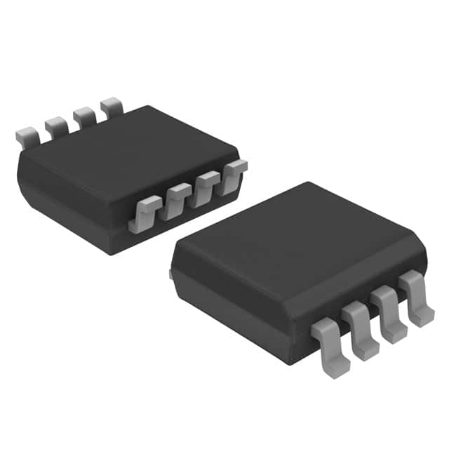
- Package: VSSOP-8
- Essence: High-performance logic gate for automotive applications
- Packaging/Quantity: Tape and Reel, 3000 pieces per reel
Specifications
- Supply Voltage Range: 1.65V to 5.5V
- Input Voltage Range: -0.5V to VCC + 0.5V
- Output Voltage Range: 0V to VCC
- Operating Temperature Range: -40°C to +125°C
- Propagation Delay: 3.9 ns (typical) at 3.3V supply, 25°C
- Quiescent Current: 10 µA (maximum) at 3.3V supply, 25°C
Detailed Pin Configuration
The 74LVC2G08DC-Q100H has a VSSOP-8 package with the following pin configuration:
____
   1 |o    |
   2 |     |
   3 |     |
   4 |     |
   5 |     |
   6 |     |
   7 |     |
   8 |____o|
Pin Description: 1. A Input 1 2. B Input 2 3. Y Output 4. GND Ground 5. NC Not Connected 6. NC Not Connected 7. VCC Power Supply 8. VCC Power Supply
Functional Features
- Dual 2-input AND gate functionality
- Low voltage CMOS technology for reduced power consumption
- Automotive grade, suitable for use in automotive applications
- Wide supply voltage range allows compatibility with various systems
- High-speed operation with low propagation delay
Advantages and Disadvantages
Advantages: - Compact VSSOP-8 package for space-constrained applications - Wide operating temperature range suitable for automotive environments - Low quiescent current for power-efficient operation - High-performance logic gate with fast propagation delay
Disadvantages: - Limited number of inputs (dual 2-input AND gate) - Not suitable for high-voltage applications
Working Principles
The 74LVC2G08DC-Q100H is a dual 2-input AND gate that performs logical AND operations on two input signals. It operates using low voltage CMOS technology, which allows for reduced power consumption. The gate is designed to meet automotive grade requirements, ensuring its reliability in automotive applications. The wide supply voltage range makes it compatible with various systems, while the high-speed operation ensures efficient signal processing.
Detailed Application Field Plans
The 74LVC2G08DC-Q100H can be used in various automotive applications where logical AND operations are required. Some potential application fields include: - Automotive control systems - Engine management systems - Body electronics - Infotainment systems - Lighting control systems
Detailed and Complete Alternative Models
- SN74LVC2G08DBVR: Dual 2-input AND gate, SOT-23-6 package
- MC74VHC1G08DTT1G: Single 2-input AND gate, SOT-363 package
- CD4081BCN: Quad 2-input AND gate, DIP-14 package
- 74HC08D: Quad 2-input AND gate, SOIC-14 package
These alternative models offer similar functionality and can be considered as substitutes for the 74LVC2G08DC-Q100H based on specific application requirements.
Word count: 410 words
Lista 10 Vanliga frågor och svar relaterade till tillämpningen av 74LVC2G08DC-Q100H i tekniska lösningar
Sure! Here are 10 common questions and answers related to the application of 74LVC2G08DC-Q100H in technical solutions:
1. What is the 74LVC2G08DC-Q100H? - The 74LVC2G08DC-Q100H is a dual 2-input AND gate IC (integrated circuit) that operates at a voltage range of 1.65V to 5.5V.
2. What is the purpose of the 74LVC2G08DC-Q100H? - The purpose of this IC is to perform logical AND operations on two input signals, providing an output signal based on their logical states.
3. What are the key features of the 74LVC2G08DC-Q100H? - Some key features include low power consumption, wide operating voltage range, high-speed operation, and compatibility with various logic families.
4. What are the typical applications of the 74LVC2G08DC-Q100H? - This IC is commonly used in digital systems, such as microcontrollers, computers, communication devices, and other electronic circuits that require logical AND operations.
5. What is the maximum operating frequency of the 74LVC2G08DC-Q100H? - The maximum operating frequency of this IC is typically around 200 MHz.
6. Can the 74LVC2G08DC-Q100H be used with different supply voltages? - Yes, it can operate within a wide voltage range of 1.65V to 5.5V, making it compatible with various power supply configurations.
7. How many inputs does the 74LVC2G08DC-Q100H have? - It has two inputs, labeled A and B, which are used for the logical AND operation.
8. What is the output voltage level of the 74LVC2G08DC-Q100H? - The output voltage level is compatible with both CMOS and TTL logic levels, typically ranging from 0V to Vcc (supply voltage).
9. Can the 74LVC2G08DC-Q100H drive other ICs directly? - Yes, it has a high output current capability, allowing it to drive other ICs or devices directly without the need for additional buffer circuits.
10. Is the 74LVC2G08DC-Q100H available in different package types? - Yes, this IC is available in various package options, such as SOT23, XSON, and DFN, providing flexibility for different PCB layouts and space constraints.
Please note that the answers provided here are general and may vary depending on specific datasheet specifications and application requirements.