

XC7SET14GV,125
Basic Information Overview
- Category: Integrated Circuit (IC)
- Use: Digital Logic Gate
- Characteristics: High-speed, Low-power consumption
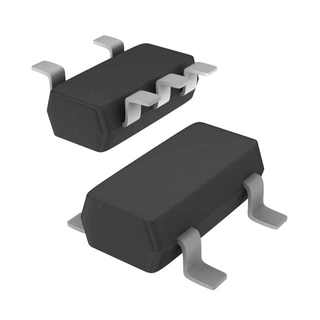
- Package: SOT-753
- Essence: Single Schmitt-Trigger Inverter
- Packaging/Quantity: Tape and Reel, 3000 pieces per reel
Specifications
- Supply Voltage Range: 1.65V to 5.5V
- Input Voltage Range: -0.5V to VCC + 0.5V
- Output Voltage Range: 0V to VCC
- Maximum Operating Frequency: 200 MHz
- Propagation Delay: 2.5 ns (typical)
Detailed Pin Configuration
The XC7SET14GV,125 has a total of five pins: 1. Pin 1: Input (A) 2. Pin 2: Ground (GND) 3. Pin 3: Output (Y) 4. Pin 4: Power Supply (VCC) 5. Pin 5: Input (A)
Functional Features
- Single Schmitt-Trigger Inverter with hysteresis
- Converts slow input signals into fast output signals
- Provides noise immunity and signal conditioning
- Suitable for applications requiring high-speed digital signal processing
Advantages
- High-speed operation allows for efficient signal processing
- Low-power consumption helps in reducing energy usage
- Noise immunity ensures reliable signal transmission
- Small package size saves board space
Disadvantages
- Limited number of inputs and outputs
- Not suitable for analog signal processing
- Requires external components for complex logic functions
Working Principles
The XC7SET14GV,125 is based on the Schmitt-trigger inverter circuit. It utilizes positive feedback to provide hysteresis, which helps in converting slow and noisy input signals into clean and fast output signals. The hysteresis ensures that the output transitions occur at different voltage levels for rising and falling input signals, providing noise immunity and preventing false triggering.
Detailed Application Field Plans
The XC7SET14GV,125 is commonly used in various digital logic applications, including: 1. Signal conditioning and level shifting 2. Clock signal generation and distribution 3. Noise filtering and glitch suppression 4. Pulse shaping and waveform generation 5. Logic signal inversion and buffering
Detailed and Complete Alternative Models
Some alternative models to XC7SET14GV,125 with similar functionality include: 1. SN74LVC1G14DBVR by Texas Instruments 2. MC74VHC1GT14DF1G by ON Semiconductor 3. 74LVC1G14GW by NXP Semiconductors 4. TC7SZ14FU by Toshiba Semiconductor
These alternatives offer comparable features and can be used as replacements based on specific application requirements.
Word count: 305 words
Lista 10 Vanliga frågor och svar relaterade till tillämpningen av XC7SET14GV,125 i tekniska lösningar
Sure! Here are 10 common questions and answers related to the application of XC7SET14GV,125 in technical solutions:
Q: What is XC7SET14GV,125? A: XC7SET14GV,125 is a specific model of FPGA (Field-Programmable Gate Array) manufactured by Xilinx.
Q: What are the key features of XC7SET14GV,125? A: Some key features of XC7SET14GV,125 include high-performance logic fabric, integrated memory blocks, DSP slices, and configurable I/Os.
Q: What are the typical applications of XC7SET14GV,125? A: XC7SET14GV,125 is commonly used in various applications such as aerospace, automotive, telecommunications, industrial automation, and medical devices.
Q: How can I program XC7SET14GV,125? A: XC7SET14GV,125 can be programmed using Xilinx's Vivado Design Suite or other compatible programming tools.
Q: What is the power supply requirement for XC7SET14GV,125? A: XC7SET14GV,125 typically operates at a voltage range of 0.95V to 1.05V, with a maximum power consumption of around 10W.
Q: Can XC7SET14GV,125 interface with other components or devices? A: Yes, XC7SET14GV,125 supports various communication protocols such as PCIe, Ethernet, USB, and SPI, allowing it to interface with other components or devices.
Q: Does XC7SET14GV,125 have built-in security features? A: Yes, XC7SET14GV,125 includes security features like bitstream encryption, authentication, and tamper detection to protect the design and data.
Q: What is the maximum operating frequency of XC7SET14GV,125? A: The maximum operating frequency of XC7SET14GV,125 depends on the specific design and implementation, but it can typically reach several hundred megahertz (MHz) or even gigahertz (GHz).
Q: Can XC7SET14GV,125 be used for real-time signal processing? A: Yes, XC7SET14GV,125's high-performance logic fabric and DSP slices make it suitable for real-time signal processing applications.
Q: Are there any development boards available for XC7SET14GV,125? A: Yes, Xilinx offers development boards like the Zynq-7000 SoC ZC702 Evaluation Kit that include XC7SET14GV,125 for prototyping and development purposes.
Please note that the specific details and answers may vary depending on the context and requirements of your technical solution.