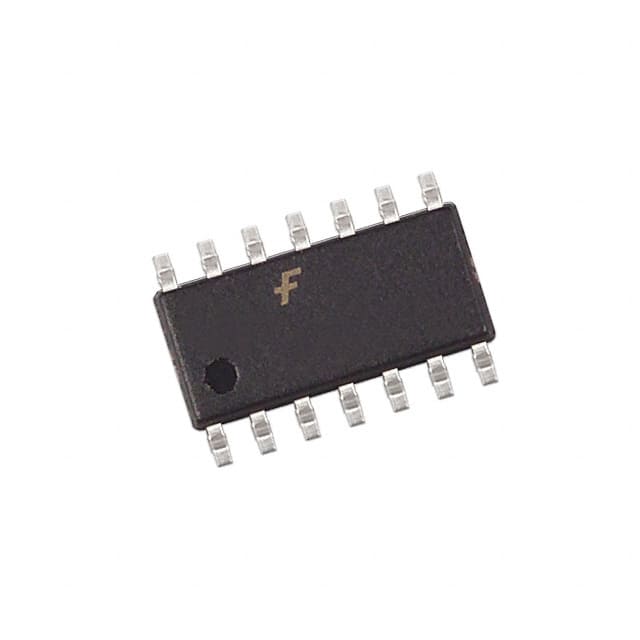
74LCX125SJ
Basic Information Overview
- Category: Integrated Circuit (IC)
- Use: Logic Level Shifter
- Characteristics: Low Voltage, High-Speed CMOS Technology
- Package: SOIC (Small Outline Integrated Circuit)
- Essence: Quad Bus Buffer Gate with 3-State Outputs
- Packaging/Quantity: Tape and Reel, 2500 pieces per reel
Specifications
- Supply Voltage Range: 1.65V to 3.6V
- Input Voltage Range: 0V to VCC
- Output Voltage Range: 0V to VCC
- Maximum Operating Frequency: 400 MHz
- Number of Inputs: 4
- Number of Outputs: 4
- Logic Family: LCX
Detailed Pin Configuration
The 74LCX125SJ has a total of 14 pins:
- Pin 1: Output 1 (Y1)
- Pin 2: Input 1 (A1)
- Pin 3: Input 2 (A2)
- Pin 4: GND (Ground)
- Pin 5: Input 3 (A3)
- Pin 6: Output Enable (OE)
- Pin 7: Output 2 (Y2)
- Pin 8: VCC (Supply Voltage)
- Pin 9: Output 3 (Y3)
- Pin 10: Input 4 (A4)
- Pin 11: Output 4 (Y4)
- Pin 12: GND (Ground)
- Pin 13: Input/Output 4 (IO4)
- Pin 14: Input/Output 3 (IO3)
Functional Features
- Quad bus buffer gate with 3-state outputs
- Provides voltage level shifting between different logic levels
- Allows bidirectional data flow
- Supports high-speed operation
- Offers low power consumption
- Provides ESD (Electrostatic Discharge) protection
Advantages and Disadvantages
Advantages: - Low voltage operation allows compatibility with various systems - High-speed CMOS technology enables fast data transmission - 3-state outputs provide flexibility in controlling bus lines
Disadvantages: - Limited number of inputs and outputs - May require additional components for complex logic operations
Working Principles
The 74LCX125SJ is a logic level shifter that operates using high-speed CMOS technology. It can shift the voltage levels between different logic families, allowing seamless communication between devices operating at different voltage levels. The device uses a quad bus buffer gate configuration with 3-state outputs, enabling bidirectional data flow. It operates within a specified supply voltage range and provides ESD protection to ensure reliable performance.
Detailed Application Field Plans
The 74LCX125SJ is commonly used in various applications, including:
- Microcontrollers: It facilitates communication between microcontrollers operating at different voltage levels.
- Communication Systems: It enables voltage level shifting in communication interfaces such as UART, SPI, and I2C.
- Data Acquisition Systems: It helps interface sensors and analog-to-digital converters with microcontrollers or digital signal processors.
- Industrial Automation: It plays a crucial role in connecting different modules and devices operating at different voltage levels in industrial automation systems.
Detailed and Complete Alternative Models
Some alternative models to the 74LCX125SJ include:
- 74LVC125A: Similar quad bus buffer gate with 3-state outputs, but operates at a wider supply voltage range.
- SN74LV1T125: Single bus buffer gate with 3-state output, suitable for low-power applications.
- CD40109B: Quad AND/OR/NAND/NOR gate with 3-state outputs, offering more logic functions.
These alternative models provide similar functionality and can be used as substitutes depending on specific requirements.
Word count: 411 words
Lista 10 Vanliga frågor och svar relaterade till tillämpningen av 74LCX125SJ i tekniska lösningar
Sure! Here are 10 common questions and answers related to the application of 74LCX125SJ in technical solutions:
Q: What is the 74LCX125SJ? A: The 74LCX125SJ is a quad buffer/line driver with 3-state outputs, commonly used in digital logic applications.
Q: What is the voltage supply range for the 74LCX125SJ? A: The 74LCX125SJ operates with a voltage supply range of 2.0V to 3.6V.
Q: How many buffers/line drivers are there in the 74LCX125SJ? A: The 74LCX125SJ has four individual buffers/line drivers.
Q: What is the purpose of the 3-state outputs in the 74LCX125SJ? A: The 3-state outputs allow the device to be connected to a bus or shared line without interfering with other devices on the same line.
Q: Can the 74LCX125SJ handle high-speed data transmission? A: Yes, the 74LCX125SJ is designed for high-speed operation and can handle fast data transmission.
Q: What is the maximum output current that the 74LCX125SJ can provide? A: The 74LCX125SJ can provide a maximum output current of 24mA per channel.
Q: Is the 74LCX125SJ compatible with both TTL and CMOS logic levels? A: Yes, the 74LCX125SJ is compatible with both TTL and CMOS logic levels, making it versatile for various applications.
Q: Can I use the 74LCX125SJ as a level shifter? A: Yes, the 74LCX125SJ can be used as a level shifter to convert signals between different voltage levels.
Q: What is the typical propagation delay of the 74LCX125SJ? A: The typical propagation delay of the 74LCX125SJ is around 3.5ns.
Q: Can I use the 74LCX125SJ in battery-powered applications? A: Yes, the 74LCX125SJ operates at low power and can be used in battery-powered applications.
Please note that these answers are general and may vary depending on specific application requirements.


