

FDD7N25LZTM
Product Overview
Category
The FDD7N25LZTM belongs to the category of power MOSFETs.
Use
It is used as a switching device in various electronic circuits and applications.
Characteristics
- High voltage capability
- Low on-resistance
- Fast switching speed
- Low gate charge
Package
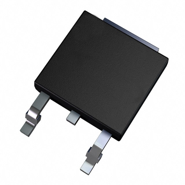
The FDD7N25LZTM is typically available in a TO-252 package.
Essence
This MOSFET is essential for controlling power flow in electronic devices and systems.
Packaging/Quantity
It is commonly packaged in reels or tubes, with quantities varying based on manufacturer specifications.
Specifications
- Drain-Source Voltage (VDS): 250V
- Continuous Drain Current (ID): 7A
- On-Resistance (RDS(on)): 0.3Ω
- Gate-Source Voltage (VGS): ±20V
- Total Gate Charge (Qg): 15nC
- Operating Temperature Range: -55°C to 150°C
Detailed Pin Configuration
The FDD7N25LZTM typically has three pins: 1. Gate (G) 2. Drain (D) 3. Source (S)
Functional Features
- High voltage capability allows for use in various power applications.
- Low on-resistance minimizes power loss and heat generation.
- Fast switching speed enables efficient control of power flow.
Advantages and Disadvantages
Advantages
- High voltage capability
- Low on-resistance
- Fast switching speed
Disadvantages
- Sensitivity to static electricity
- Limited maximum operating temperature
Working Principles
The FDD7N25LZTM operates based on the principles of field-effect transistors, where the voltage applied to the gate terminal controls the flow of current between the drain and source terminals.
Detailed Application Field Plans
The FDD7N25LZTM is widely used in the following applications: - Switching power supplies - Motor control - LED lighting - Audio amplifiers - Automotive electronics
Detailed and Complete Alternative Models
Some alternative models to the FDD7N25LZTM include: - IRF540N - FQP30N06L - STP80NF55-06
In conclusion, the FDD7N25LZTM is a high-voltage power MOSFET with characteristics that make it suitable for a wide range of electronic applications, despite its limitations. Its functional features, advantages, and detailed application field plans demonstrate its significance in the realm of power electronics.
[Word count: 344]
Lista 10 Vanliga frågor och svar relaterade till tillämpningen av FDD7N25LZTM i tekniska lösningar
What is the maximum drain-source voltage of FDD7N25LZTM?
- The maximum drain-source voltage of FDD7N25LZTM is 250V.
What is the continuous drain current rating of FDD7N25LZTM?
- The continuous drain current rating of FDD7N25LZTM is 7A.
What is the on-resistance of FDD7N25LZTM?
- The on-resistance of FDD7N25LZTM is typically 0.18 ohms.
Can FDD7N25LZTM be used for switching applications?
- Yes, FDD7N25LZTM is suitable for switching applications due to its low on-resistance and high voltage rating.
What is the gate-source threshold voltage of FDD7N25LZTM?
- The gate-source threshold voltage of FDD7N25LZTM is typically 2V.
Is FDD7N25LZTM suitable for use in automotive applications?
- Yes, FDD7N25LZTM is designed for automotive applications and meets relevant industry standards.
Does FDD7N25LZTM require a heat sink for operation?
- The need for a heat sink depends on the specific application and power dissipation requirements. It's recommended to consult the datasheet for thermal considerations.
What are the typical applications for FDD7N25LZTM?
- Typical applications for FDD7N25LZTM include motor control, power management, and automotive systems.
What is the operating temperature range of FDD7N25LZTM?
- FDD7N25LZTM has an operating temperature range of -55°C to 150°C.
Is FDD7N25LZTM RoHS compliant?
- Yes, FDD7N25LZTM is RoHS compliant, making it suitable for environmentally conscious designs.