

FDW254P Product Overview
Introduction
The FDW254P is a versatile electronic component that belongs to the category of integrated circuits. This semiconductor device is widely used in various electronic applications due to its unique characteristics and functional features.
Basic Information Overview
- Category: Integrated Circuit
- Use: Signal Processing, Amplification, Control Circuits
- Characteristics: High Gain, Low Power Consumption, Small Footprint
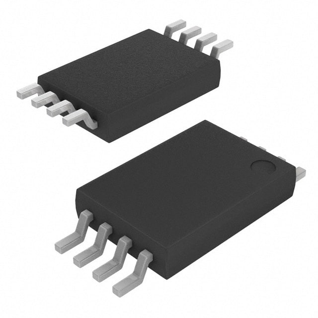
- Package: DIP (Dual Inline Package), SOIC (Small Outline Integrated Circuit)
- Essence: Amplification and Signal Conditioning
- Packaging/Quantity: Typically supplied in reels or tubes containing 50 to 100 units per package.
Specifications
- Operating Voltage: 3V to 15V
- Operating Temperature: -40°C to 85°C
- Gain Bandwidth Product: 1MHz
- Input Offset Voltage: 2mV
- Output Current: 20mA
Detailed Pin Configuration
The FDW254P has a standard pin configuration with 8 pins arranged in a dual inline package. The pinout is as follows: 1. VCC (Power Supply) 2. Inverting Input 3. Non-Inverting Input 4. Ground 5. Output 6. Compensation 7. NC (No Connection) 8. VEE (Negative Power Supply)
Functional Features
- High Gain: The FDW254P offers a high voltage gain, making it suitable for amplification applications.
- Low Power Consumption: This integrated circuit is designed to operate efficiently with minimal power consumption, making it suitable for battery-powered devices.
- Small Footprint: The compact package size allows for space-efficient PCB layout and integration into small form factor designs.
Advantages and Disadvantages
Advantages
- Versatile Application: Suitable for a wide range of signal processing and control circuit applications.
- Low Noise: Provides clean and accurate signal amplification with minimal noise interference.
- Cost-Effective: Offers a cost-effective solution for electronic circuit design and manufacturing.
Disadvantages
- Limited Output Current: The maximum output current may be insufficient for high-power applications.
- Sensitivity to ESD: Requires careful handling to prevent damage from electrostatic discharge.
Working Principles
The FDW254P operates based on the principles of operational amplifiers, utilizing differential input signals to produce amplified output signals. It incorporates internal compensation and biasing circuits to ensure stable and reliable operation within specified operating conditions.
Detailed Application Field Plans
The FDW254P finds extensive use in the following application fields: - Audio Amplification: Used in audio preamplifiers and equalization circuits. - Sensor Signal Conditioning: Employed in sensor interface circuits for amplifying and conditioning sensor outputs. - Control Circuits: Integrated into control systems for precision signal processing and feedback control.
Detailed and Complete Alternative Models
- FDW255P: A higher-gain version of the FDW254P with similar pin configuration and package options.
- FDW253P: A lower-power version of the FDW254P suitable for low-power applications.
In conclusion, the FDW254P integrated circuit offers a balance of performance, versatility, and cost-effectiveness, making it a popular choice for various electronic applications.
Word Count: 489
Lista 10 Vanliga frågor och svar relaterade till tillämpningen av FDW254P i tekniska lösningar
What is FDW254P?
- FDW254P is a high-performance electronic component used in technical solutions, particularly in power electronics and control systems.
What are the key features of FDW254P?
- The key features of FDW254P include high voltage capability, low on-resistance, fast switching speed, and robustness for demanding applications.
How is FDW254P typically used in technical solutions?
- FDW254P is commonly used in applications such as motor control, power supplies, inverters, and other high-power electronic systems.
What are the advantages of using FDW254P in technical solutions?
- Using FDW254P can lead to improved energy efficiency, reduced heat dissipation, and enhanced overall performance of the electronic system.
Are there any specific design considerations when using FDW254P?
- Designers need to consider proper thermal management, gate drive requirements, and protection circuitry to maximize the benefits of FDW254P in their technical solutions.
What are the typical operating conditions for FDW254P?
- FDW254P operates under a wide range of voltages and temperatures, making it suitable for various industrial and automotive applications.
Can FDW254P be used in high-frequency applications?
- Yes, FDW254P is designed to operate effectively in high-frequency switching applications, making it versatile for different technical solutions.
Are there any recommended alternative components to FDW254P?
- While there are alternatives available, FDW254P is often preferred due to its specific combination of performance characteristics and reliability.
What are the potential challenges when integrating FDW254P into a technical solution?
- Challenges may include optimizing the driving circuitry, managing EMI/EMC issues, and ensuring compatibility with other system components.
Where can I find detailed technical specifications and application notes for FDW254P?
- Detailed technical specifications and application notes for FDW254P can be found on the manufacturer's website or through authorized distributors.