

NL17SZ06XV5T2G
Basic Information Overview
- Category: Integrated Circuit (IC)
- Use: Logic Gate
- Characteristics: Single Schmitt-Trigger Inverter
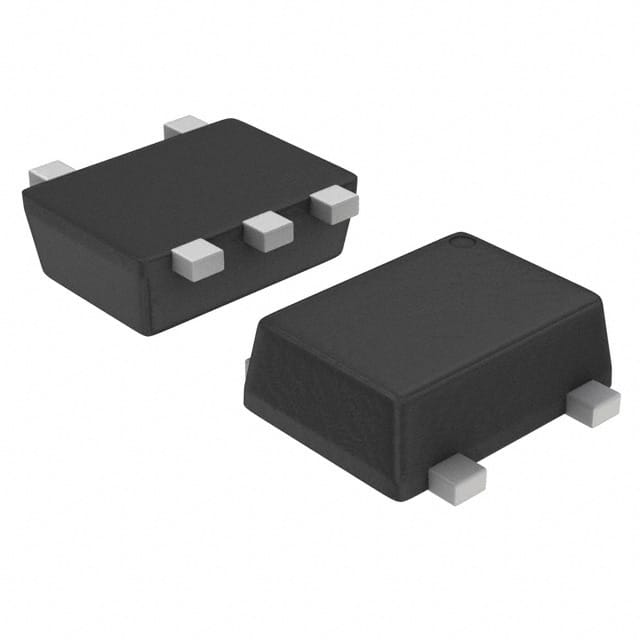
- Package: SOT-353
- Essence: High-speed CMOS technology
- Packaging/Quantity: Tape and Reel, 3000 pieces per reel
Specifications
- Supply Voltage Range: 1.65V to 5.5V
- Input Voltage Range: 0V to VCC
- Output Voltage Range: 0V to VCC
- Maximum Operating Frequency: 200MHz
- Propagation Delay Time: 3.8ns (typical) at 5V supply voltage
- Input Capacitance: 1.5pF (typical)
Detailed Pin Configuration
The NL17SZ06XV5T2G has a total of 5 pins: 1. GND (Ground): Connected to the ground reference potential. 2. IN (Input): Accepts the input logic signal. 3. OUT (Output): Provides the inverted output logic signal. 4. VCC (Supply Voltage): Connected to the positive supply voltage. 5. NC (No Connection): This pin is not connected internally and can be left unconnected.
Functional Features
- Single Schmitt-Trigger Inverter: Converts input logic levels into inverted logic levels with hysteresis.
- High-Speed Operation: Capable of operating at frequencies up to 200MHz.
- Wide Supply Voltage Range: Can operate from 1.65V to 5.5V, making it suitable for various applications.
- Low Power Consumption: Consumes minimal power during operation.
- Small Package Size: The SOT-353 package offers compactness and ease of integration.
Advantages and Disadvantages
Advantages: - Fast switching speed enables high-speed data processing. - Wide supply voltage range allows compatibility with different systems. - Low power consumption contributes to energy efficiency. - Small package size facilitates space-constrained designs.
Disadvantages: - Limited number of logic gates in a single IC package. - May require additional components for certain applications.
Working Principles
The NL17SZ06XV5T2G is based on high-speed CMOS technology. It utilizes a Schmitt-trigger circuit to provide hysteresis, which helps in reducing noise and improving the robustness of the input signal. When the input voltage crosses a certain threshold, the output switches states, providing an inverted logic level.
Detailed Application Field Plans
The NL17SZ06XV5T2G can be used in various applications, including but not limited to: 1. Digital Communication Systems: Signal inversion and level shifting. 2. Microcontrollers and Microprocessors: Logic level conversion and interfacing. 3. Industrial Automation: Sensor signal conditioning and interfacing. 4. Consumer Electronics: Signal processing and control circuits. 5. Automotive Electronics: ECU (Engine Control Unit) and sensor interface circuits.
Detailed and Complete Alternative Models
- SN74LVC1G04DBVR: Single Inverter Gate, SOT-23 package.
- MC74VHC1G14DFT1G: Single Schmitt-Trigger Inverter, SOT-353 package.
- CD40106BE: Hex Schmitt-Trigger Inverter, DIP-14 package.
- 74HCT04N: Hex Inverter, DIP-14 package.
- TC7SZ04FU: Single Inverter Gate, SOT-353 package.
(Note: The above list is not exhaustive and serves as examples of alternative models.)
This entry provides comprehensive information about the NL17SZ06XV5T2G integrated circuit. It includes the product's basic information, specifications, pin configuration, functional features, advantages and disadvantages, working principles, application field plans, and alternative models.
Lista 10 Vanliga frågor och svar relaterade till tillämpningen av NL17SZ06XV5T2G i tekniska lösningar
Sure! Here are 10 common questions and answers related to the application of NL17SZ06XV5T2G in technical solutions:
Q: What is NL17SZ06XV5T2G? A: NL17SZ06XV5T2G is a specific type of logic gate, specifically a single inverter gate, commonly used in digital circuits.
Q: What is the purpose of NL17SZ06XV5T2G in technical solutions? A: NL17SZ06XV5T2G is used to invert or complement digital signals, which can be useful for various applications such as signal conditioning, level shifting, and waveform generation.
Q: What voltage levels does NL17SZ06XV5T2G support? A: NL17SZ06XV5T2G typically supports a wide range of voltage levels, including both TTL (Transistor-Transistor Logic) and CMOS (Complementary Metal-Oxide-Semiconductor) voltage levels.
Q: Can NL17SZ06XV5T2G be used in high-speed applications? A: Yes, NL17SZ06XV5T2G is designed to operate at high speeds, making it suitable for applications that require fast switching times.
Q: How many inputs and outputs does NL17SZ06XV5T2G have? A: NL17SZ06XV5T2G has one input and one output. It is a single-channel device.
Q: What is the power supply requirement for NL17SZ06XV5T2G? A: NL17SZ06XV5T2G typically operates with a power supply voltage ranging from 1.65V to 5.5V, depending on the specific variant.
Q: Can NL17SZ06XV5T2G be used in battery-powered applications? A: Yes, NL17SZ06XV5T2G's low power consumption and wide voltage range make it suitable for battery-powered applications.
Q: Is NL17SZ06XV5T2G available in different package options? A: Yes, NL17SZ06XV5T2G is available in various package options, such as SOT-23 and SC-70, allowing flexibility in design and integration.
Q: Can NL17SZ06XV5T2G be used in both digital and analog circuits? A: NL17SZ06XV5T2G is primarily designed for digital circuits, but it can also be used in certain analog applications where signal inversion is required.
Q: Are there any specific precautions to consider when using NL17SZ06XV5T2G? A: It is important to follow the manufacturer's datasheet and guidelines for proper usage, including considerations for voltage levels, current limitations, and temperature ranges to ensure reliable operation.
Please note that the answers provided here are general and may vary based on the specific application and requirements. Always refer to the manufacturer's documentation for accurate and detailed information.