

NL17VHC1G07DTT1G
Basic Information Overview
- Category: Integrated Circuit (IC)
- Use: Logic Gate
- Characteristics: High-speed, Low-power consumption
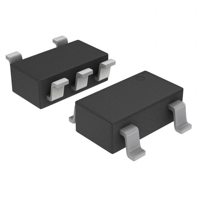
- Package: SOT-353
- Essence: Single Buffer/Driver
- Packaging/Quantity: Tape and Reel, 3000 pieces per reel
Specifications
- Supply Voltage Range: 2.0V to 5.5V
- Input Voltage Range: 0V to VCC
- Output Voltage Range: 0V to VCC
- Operating Temperature Range: -40°C to +125°C
- Propagation Delay Time: 3.8ns (typical)
- Maximum Quiescent Current: 1μA
Detailed Pin Configuration
The NL17VHC1G07DTT1G has the following pin configuration:
____
   A -|    |- VCC
   B -|    |- Y
 GND -|____|- /Y
Functional Features
- Single buffer/driver with open-drain output
- Compatible with TTL and CMOS logic levels
- High-speed operation with low propagation delay
- Low power consumption
- Wide supply voltage range for versatile applications
- ESD protection on all pins
Advantages and Disadvantages
Advantages: - High-speed operation allows for efficient data transmission - Low power consumption extends battery life in portable devices - Versatile supply voltage range enables compatibility with various systems - ESD protection ensures robustness against electrostatic discharge
Disadvantages: - Open-drain output requires external pull-up resistor for proper signal level translation - Limited number of input/output pins restricts complex circuit designs
Working Principles
The NL17VHC1G07DTT1G is a single buffer/driver IC that provides a logic level translation function. It takes an input signal and amplifies it to drive an open-drain output. The open-drain configuration allows for easy interfacing with other devices by connecting the output to a pull-up resistor. When the input is low, the output is pulled low, and when the input is high, the output is in a high-impedance state.
Detailed Application Field Plans
The NL17VHC1G07DTT1G can be used in various applications, including:
- Communication Systems: Signal level translation between different voltage domains in data communication interfaces.
- Industrial Control: Interface between microcontrollers and peripheral devices, such as sensors and actuators.
- Automotive Electronics: Logic level conversion for automotive control units and communication buses.
- Consumer Electronics: Voltage level shifting in audio/video equipment, gaming consoles, and home automation systems.
- Medical Devices: Signal conditioning and level translation in medical monitoring and diagnostic equipment.
Detailed and Complete Alternative Models
- SN74LVC1G07DBVR - Single Buffer/Driver IC from Texas Instruments
- MC74VHC1GT07DF1G - Single Buffer/Driver IC from ON Semiconductor
- 74LVC1G07GW - Single Buffer/Driver IC from NXP Semiconductors
- TC7SZ07FU - Single Buffer/Driver IC from Toshiba Semiconductor
These alternative models offer similar functionality and can be considered as replacements for the NL17VHC1G07DTT1G in various applications.
Word count: 400 words
Lista 10 Vanliga frågor och svar relaterade till tillämpningen av NL17VHC1G07DTT1G i tekniska lösningar
Sure! Here are 10 common questions and answers related to the application of NL17VHC1G07DTT1G in technical solutions:
Q1: What is NL17VHC1G07DTT1G? A1: NL17VHC1G07DTT1G is a specific type of logic gate, specifically an open-drain buffer, which can be used in various technical solutions.
Q2: What is the purpose of NL17VHC1G07DTT1G? A2: The purpose of NL17VHC1G07DTT1G is to provide voltage level shifting and buffering capabilities in digital circuits.
Q3: What voltage levels does NL17VHC1G07DTT1G support? A3: NL17VHC1G07DTT1G supports voltage levels ranging from 1.65V to 5.5V.
Q4: How many inputs and outputs does NL17VHC1G07DTT1G have? A4: NL17VHC1G07DTT1G has one input and one output.
Q5: Can NL17VHC1G07DTT1G be used for bidirectional communication? A5: No, NL17VHC1G07DTT1G is unidirectional and can only be used for one-way data transmission.
Q6: What is the maximum frequency at which NL17VHC1G07DTT1G can operate? A6: NL17VHC1G07DTT1G can operate at a maximum frequency of 200 MHz.
Q7: Is NL17VHC1G07DTT1G compatible with other logic families? A7: Yes, NL17VHC1G07DTT1G is compatible with a wide range of logic families, including CMOS, TTL, and LVCMOS.
Q8: Can NL17VHC1G07DTT1G be used in battery-powered applications? A8: Yes, NL17VHC1G07DTT1G is suitable for battery-powered applications as it has low power consumption.
Q9: What are the typical applications of NL17VHC1G07DTT1G? A9: NL17VHC1G07DTT1G is commonly used in level shifting, voltage translation, and interfacing between different logic levels.
Q10: Is NL17VHC1G07DTT1G available in different package options? A10: Yes, NL17VHC1G07DTT1G is available in various package options, such as SOT-23 and SC-70, to suit different design requirements.
Please note that these answers are general and may vary depending on specific technical requirements and datasheet specifications.