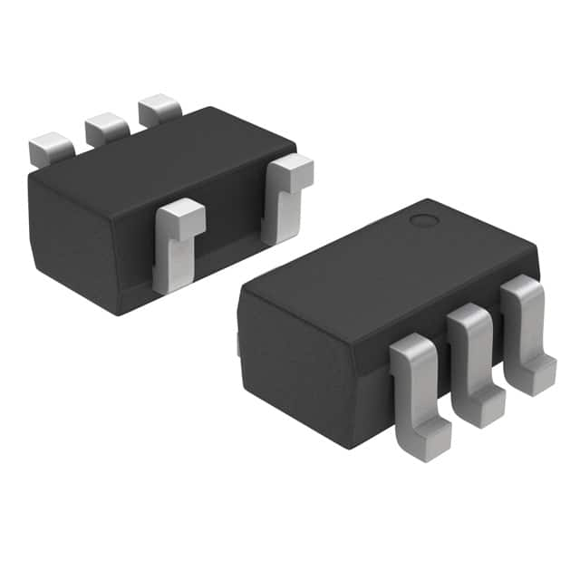
NLAS4501DFT2G
Product Overview
Category: Integrated Circuit (IC)
Use: The NLAS4501DFT2G is a high-performance analog switch designed for use in various electronic applications. It provides a versatile solution for signal routing and switching in both digital and analog circuits.
Characteristics: - Low ON-resistance - Wide voltage range compatibility - High bandwidth - Low power consumption - Small package size
Package: The NLAS4501DFT2G is available in a compact surface-mount package, making it suitable for space-constrained designs.
Essence: This IC serves as a reliable and efficient component for signal switching and routing within electronic systems.
Packaging/Quantity: The NLAS4501DFT2G is typically packaged in reels or tubes, with quantities varying based on customer requirements.
Specifications
- Supply Voltage Range: 1.65V to 5.5V
- ON-Resistance (RON): 0.6Ω (typical)
- Bandwidth: Up to 400MHz
- Leakage Current (ILEAK): 1nA (maximum)
- Control Input Voltage Range: 0V to VCC
- Operating Temperature Range: -40°C to +85°C
Detailed Pin Configuration
The NLAS4501DFT2G features a standard pin configuration with the following connections:
- Pin 1: Control Input (IN)
- Pin 2: Source (S)
- Pin 3: Drain (D)
- Pin 4: Ground (GND)
- Pin 5: Control Input (IN)
- Pin 6: Drain (D)
- Pin 7: Source (S)
- Pin 8: VCC (Supply Voltage)
Functional Features
- Low ON-resistance ensures minimal signal distortion and power loss.
- Wide voltage range compatibility allows for versatile integration with various systems.
- High bandwidth enables efficient transmission of high-frequency signals.
- Low power consumption contributes to energy-efficient designs.
- Compact package size facilitates space-saving circuit layouts.
Advantages and Disadvantages
Advantages: - Reliable signal routing and switching capabilities - Versatile compatibility with different voltage levels - High-speed performance for demanding applications - Low power consumption for energy-efficient designs - Compact package size for space-constrained applications
Disadvantages: - Limited current handling capacity - Sensitivity to electrostatic discharge (ESD) - May require additional protection circuitry in certain applications
Working Principles
The NLAS4501DFT2G operates based on the principle of a metal-oxide-semiconductor field-effect transistor (MOSFET). It utilizes a control input voltage to toggle between an open and closed state, allowing or blocking the flow of signals between the source and drain terminals. The low ON-resistance ensures minimal signal attenuation and distortion during switching operations.
Detailed Application Field Plans
The NLAS4501DFT2G finds application in various electronic systems, including but not limited to: - Audio and video equipment - Communication devices - Test and measurement instruments - Industrial automation systems - Consumer electronics
Detailed and Complete Alternative Models
- NLAS4501DFT2G is part of the NLAS series from ON Semiconductor, which includes other models such as NLAS4599DFT2G, NLAS4684DFT2G, and NLAS4717DFT2G.
- Alternative manufacturers offering similar analog switches include Texas Instruments (TS5A23157), Maxim Integrated (MAX4544), and Analog Devices (ADG1414).
Note: The above list is not exhaustive and serves as a reference for alternative models.
Word Count: 439 words
Lista 10 Vanliga frågor och svar relaterade till tillämpningen av NLAS4501DFT2G i tekniska lösningar
Sure! Here are 10 common questions and answers related to the application of NLAS4501DFT2G in technical solutions:
Q1: What is NLAS4501DFT2G? A1: NLAS4501DFT2G is a specific model number for a digital switch IC (integrated circuit) manufactured by ON Semiconductor.
Q2: What is the purpose of NLAS4501DFT2G? A2: The NLAS4501DFT2G is designed to function as a high-speed, low-power, bidirectional analog switch for various applications.
Q3: What are some typical applications of NLAS4501DFT2G? A3: NLAS4501DFT2G can be used in audio and video signal routing, data acquisition systems, test and measurement equipment, and other similar applications.
Q4: What is the voltage range supported by NLAS4501DFT2G? A4: NLAS4501DFT2G supports a wide voltage range from -0.5V to +5.5V, making it suitable for both single-supply and dual-supply systems.
Q5: What is the maximum current handling capability of NLAS4501DFT2G? A5: NLAS4501DFT2G can handle a maximum continuous current of 200mA, which makes it suitable for many low-power applications.
Q6: Does NLAS4501DFT2G have built-in ESD protection? A6: Yes, NLAS4501DFT2G has built-in ESD (Electrostatic Discharge) protection, ensuring robustness against static electricity.
Q7: Can NLAS4501DFT2G operate at high frequencies? A7: Yes, NLAS4501DFT2G is designed to operate at high frequencies, making it suitable for applications that require fast switching.
Q8: Is NLAS4501DFT2G compatible with both CMOS and TTL logic levels? A8: Yes, NLAS4501DFT2G is compatible with both CMOS (Complementary Metal-Oxide-Semiconductor) and TTL (Transistor-Transistor Logic) logic levels.
Q9: Does NLAS4501DFT2G have a low on-resistance? A9: Yes, NLAS4501DFT2G has a low on-resistance of typically 4 ohms, which helps minimize signal distortion.
Q10: Can NLAS4501DFT2G be used in battery-powered devices? A10: Yes, NLAS4501DFT2G is suitable for battery-powered devices due to its low power consumption and wide voltage range support.
Please note that the answers provided here are general and may vary depending on specific application requirements.


