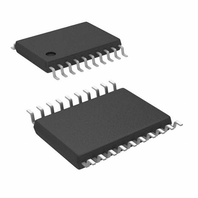
NLVHCT244ADTR2G
Basic Information Overview
- Category: Integrated Circuit (IC)
- Use: Buffer/Line Driver
- Characteristics: High-speed, low-voltage, octal buffer with 3-state outputs
- Package: TSSOP-20
- Essence: Provides voltage level shifting and signal buffering capabilities
- Packaging/Quantity: Tape and Reel, 2500 units per reel
Specifications
- Supply Voltage Range: 1.65V to 5.5V
- Logic Family: CMOS
- Number of Channels: 8
- Output Type: 3-State
- Input/Output Compatibility: TTL, LVTTL, LVCMOS
- Operating Temperature Range: -40°C to +85°C
- Propagation Delay: 4.5ns (typical)
- Output Drive Capability: ±24mA
Detailed Pin Configuration
- A1 - Input/Output 1
- Y1 - Output 1
- GND - Ground
- A2 - Input/Output 2
- Y2 - Output 2
- A3 - Input/Output 3
- Y3 - Output 3
- VCC - Power Supply
- Y4 - Output 4
- A4 - Input/Output 4
- Y5 - Output 5
- A5 - Input/Output 5
- Y6 - Output 6
- A6 - Input/Output 6
- Y7 - Output 7
- A7 - Input/Output 7
- Y8 - Output 8
- OE - Output Enable
- A8 - Input/Output 8
- GND - Ground
Functional Features
- High-speed operation allows for efficient signal transmission.
- Low-voltage capability enables compatibility with various logic families.
- 3-state outputs provide flexibility in controlling signal flow.
- Wide supply voltage range allows for versatile applications.
- Output drive capability supports driving of external loads.
Advantages
- Versatile voltage level shifting and buffering solution.
- Suitable for low-power and portable electronic devices.
- High-speed operation enhances system performance.
- Compact TSSOP package saves board space.
- 3-state outputs enable bus sharing and multiplexing.
Disadvantages
- Limited output drive capability may not be suitable for high-current applications.
- Not compatible with all logic families, requiring level translation in some cases.
- Sensitivity to electrostatic discharge (ESD) requires proper handling during assembly.
Working Principles
The NLVHCT244ADTR2G is an octal buffer IC that operates by receiving input signals on the A1-A8 pins. These signals are then amplified and buffered internally before being transmitted to the corresponding Y1-Y8 output pins. The OE pin controls the output enable/disable function, allowing the user to control the signal flow. The CMOS technology used in this IC ensures low power consumption and high noise immunity.
Detailed Application Field Plans
- Level shifting between different logic families (TTL, LVTTL, LVCMOS).
- Signal buffering in communication systems.
- Bus sharing and multiplexing in digital circuits.
- Interface conversion in mixed-signal systems.
- Buffering and line driving in data acquisition systems.
Detailed and Complete Alternative Models
- SN74LV244A: Similar octal buffer IC with 3-state outputs, available in different packages.
- MC74LVX244: Octal buffer IC with 3-state outputs, compatible with wider supply voltage range.
- CD74HC244: Octal buffer IC with 3-state outputs, suitable for high-speed applications.
- 74HCT244: Octal buffer IC with 3-state outputs, compatible with TTL logic levels.
(Note: The alternative models listed above are just a few examples and not an exhaustive list.)
Word Count: 420
Lista 10 Vanliga frågor och svar relaterade till tillämpningen av NLVHCT244ADTR2G i tekniska lösningar
Sure! Here are 10 common questions and answers related to the application of NLVHCT244ADTR2G in technical solutions:
Question: What is NLVHCT244ADTR2G?
- Answer: NLVHCT244ADTR2G is a specific type of integrated circuit (IC) that belongs to the HCT family of logic gates. It is a non-inverting buffer/line driver with 3-state outputs.Question: What is the purpose of NLVHCT244ADTR2G in technical solutions?
- Answer: NLVHCT244ADTR2G is commonly used as a buffer or line driver to amplify and shape digital signals, ensuring proper signal integrity and driving capability in various electronic systems.Question: What voltage levels does NLVHCT244ADTR2G support?
- Answer: NLVHCT244ADTR2G operates at a supply voltage range of 2 V to 5.5 V, making it compatible with both low-voltage and standard CMOS logic levels.Question: Can NLVHCT244ADTR2G handle bidirectional data flow?
- Answer: No, NLVHCT244ADTR2G is a unidirectional buffer, meaning it can only drive signals in one direction. For bidirectional data flow, you would need to use a different IC or employ additional circuitry.Question: What is the maximum output current of NLVHCT244ADTR2G?
- Answer: The maximum output current that NLVHCT244ADTR2G can source or sink is typically around 8 mA, which is sufficient for most digital applications.Question: Can NLVHCT244ADTR2G tolerate overvoltage or undervoltage conditions?
- Answer: NLVHCT244ADTR2G has built-in protection features that allow it to tolerate limited overvoltage and undervoltage conditions, but it is always recommended to operate within the specified voltage range for optimal performance and reliability.Question: What is the propagation delay of NLVHCT244ADTR2G?
- Answer: The propagation delay, which refers to the time taken for a signal to propagate through the IC, is typically in the range of a few nanoseconds for NLVHCT244ADTR2G.Question: Can NLVHCT244ADTR2G be used in high-speed applications?
- Answer: While NLVHCT244ADTR2G is not specifically designed for high-speed applications, it can still be used in moderate-speed digital systems where the propagation delay and switching speed requirements are not extremely critical.Question: Is NLVHCT244ADTR2G available in different package options?
- Answer: Yes, NLVHCT244ADTR2G is available in various package options, including surface mount packages like TSSOP (Thin Shrink Small Outline Package) and SOIC (Small Outline Integrated Circuit).Question: Are there any specific precautions to consider when using NLVHCT244ADTR2G?
- Answer: It is important to ensure proper decoupling capacitors are used near the power supply pins of NLVHCT244ADTR2G to minimize noise and voltage fluctuations. Additionally, care should be taken to avoid exceeding the maximum operating temperature and voltage limits specified in the datasheet.


