

NLX2GU04BMX1TCG
Product Overview
Category: Integrated Circuit (IC)
Use: Logic Gate
Characteristics: - High-speed operation - Low power consumption - Small package size - Wide operating voltage range
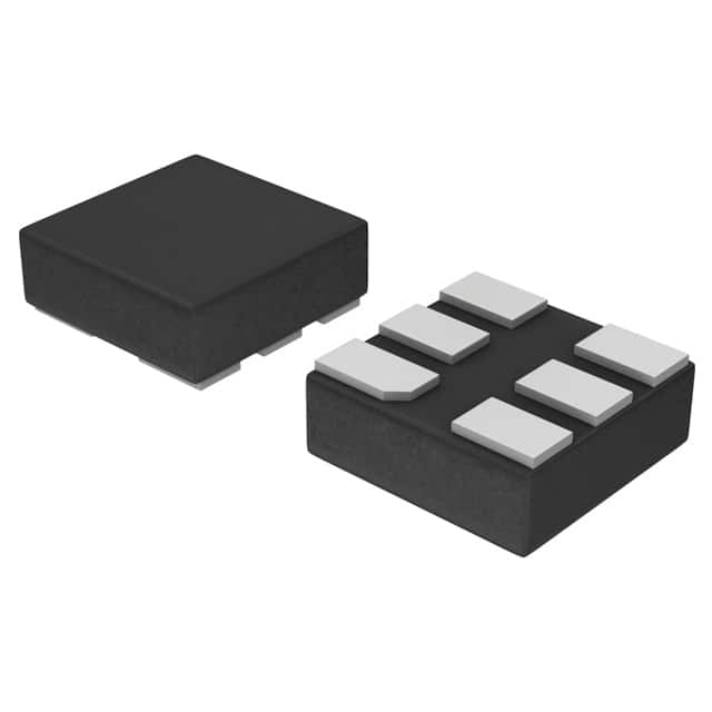
Package: SOT-23-5
Essence: The NLX2GU04BMX1TCG is a logic gate IC that provides high-speed operation and low power consumption. It is commonly used in digital circuits for signal processing and logical operations.
Packaging/Quantity: The NLX2GU04BMX1TCG is typically packaged in a SOT-23-5 package, which contains 3000 units per reel.
Specifications
- Supply Voltage Range: 1.65V to 5.5V
- Input Voltage Range: 0V to VCC
- Output Voltage Range: 0V to VCC
- Operating Temperature Range: -40°C to +85°C
- Propagation Delay Time: 3.5ns (typical)
- Maximum Quiescent Current: 1μA (at 5.5V)
Detailed Pin Configuration
The NLX2GU04BMX1TCG has a total of 5 pins:
- GND (Ground): Connected to the ground reference of the circuit.
- A (Input): First input pin for the logic gate.
- Y (Output): Output pin of the logic gate.
- B (Input): Second input pin for the logic gate.
- VCC (Supply Voltage): Connected to the positive supply voltage of the circuit.
Functional Features
- Inverter Function: The NLX2GU04BMX1TCG acts as an inverter, producing the complement of the input signal at the output.
- High-Speed Operation: The IC operates at high speeds, making it suitable for applications that require fast signal processing.
- Low Power Consumption: The NLX2GU04BMX1TCG consumes minimal power, making it energy-efficient and suitable for battery-powered devices.
Advantages and Disadvantages
Advantages: - High-speed operation enables quick signal processing. - Low power consumption prolongs battery life in portable devices. - Small package size allows for space-saving circuit designs. - Wide operating voltage range provides flexibility in various applications.
Disadvantages: - Limited functionality as it only performs the inverter function. - Not suitable for applications requiring complex logical operations.
Working Principles
The NLX2GU04BMX1TCG is based on complementary metal-oxide-semiconductor (CMOS) technology. It utilizes a combination of NMOS and PMOS transistors to implement the inverter function. When the input signal is high, the PMOS transistor turns off, while the NMOS transistor turns on, resulting in a low output. Conversely, when the input signal is low, the PMOS transistor turns on, and the NMOS transistor turns off, producing a high output.
Detailed Application Field Plans
The NLX2GU04BMX1TCG is commonly used in various digital circuits and systems, including but not limited to: - Microcontrollers - Digital signal processors - Communication systems - Consumer electronics - Industrial automation
Detailed and Complete Alternative Models
Some alternative models to the NLX2GU04BMX1TCG include: - SN74LVC1G04DBVR - MC74VHC1G04DFT1G - 74AUP1G04GW
These alternative models offer similar functionality and characteristics, providing options for designers based on specific requirements and availability.
Word count: 410 words
Lista 10 Vanliga frågor och svar relaterade till tillämpningen av NLX2GU04BMX1TCG i tekniska lösningar
Sure! Here are 10 common questions and answers related to the application of NLX2GU04BMX1TCG in technical solutions:
Q1: What is NLX2GU04BMX1TCG? A1: NLX2GU04BMX1TCG is a specific type of integrated circuit (IC) that consists of six inverters. It is commonly used in various technical solutions.
Q2: What is the purpose of NLX2GU04BMX1TCG? A2: The purpose of NLX2GU04BMX1TCG is to provide signal inversion functionality, making it useful for voltage level shifting, signal buffering, and other applications.
Q3: What is the operating voltage range of NLX2GU04BMX1TCG? A3: NLX2GU04BMX1TCG operates within a voltage range of typically 1.65V to 5.5V, making it compatible with a wide range of systems.
Q4: Can NLX2GU04BMX1TCG be used in low-power applications? A4: Yes, NLX2GU04BMX1TCG is designed to operate at low power consumption levels, making it suitable for battery-powered devices and energy-efficient applications.
Q5: Is NLX2GU04BMX1TCG suitable for high-speed data transmission? A5: While NLX2GU04BMX1TCG can handle moderate data rates, it is not specifically optimized for high-speed data transmission. Other specialized ICs may be more suitable for such applications.
Q6: Can NLX2GU04BMX1TCG be used in both digital and analog circuits? A6: NLX2GU04BMX1TCG is primarily designed for digital applications, but it can also be used in certain analog circuits where signal inversion is required.
Q7: What is the package type of NLX2GU04BMX1TCG? A7: NLX2GU04BMX1TCG is typically available in a small surface-mount package, such as a 14-pin TSSOP (Thin Shrink Small Outline Package).
Q8: Are there any temperature limitations for NLX2GU04BMX1TCG? A8: NLX2GU04BMX1TCG has an operating temperature range of typically -40°C to +85°C, allowing it to function reliably in a wide range of environments.
Q9: Can NLX2GU04BMX1TCG be cascaded or connected in series? A9: Yes, multiple NLX2GU04BMX1TCG ICs can be cascaded or connected in series to achieve more complex logic functions or to increase the number of inverters.
Q10: Where can I find more information about using NLX2GU04BMX1TCG in technical solutions? A10: You can refer to the datasheet provided by the manufacturer of NLX2GU04BMX1TCG for detailed information on its electrical characteristics, recommended usage, and application examples.