

Encyclopedia Entry: 74V1G125STR
Product Information Overview
- Category: Integrated Circuit (IC)
- Use: Buffer/Driver
- Characteristics: High-speed, low-power, single gate, non-inverting buffer/driver
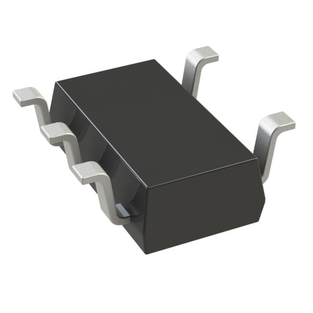
- Package: SOT-23-5
- Essence: The 74V1G125STR is a versatile IC that provides buffering and driving capabilities for digital signals.
- Packaging/Quantity: Available in tape and reel packaging with 3000 units per reel.
Specifications
- Supply Voltage: 1.65V to 5.5V
- Input Voltage Range: 0V to VCC
- Output Voltage Range: 0V to VCC
- Operating Temperature Range: -40°C to +85°C
- Propagation Delay: 3.5ns (typical)
- Output Current: ±8mA
- Input Capacitance: 2pF (typical)
Detailed Pin Configuration
The 74V1G125STR IC has a total of 5 pins arranged as follows:
____
   Y1 |    | VCC
   A1 |    | GND
   OE |    | Y2
   A2 |    |
   GND|____|
- A1, A2: Input pins for the digital signal to be buffered or driven.
- Y1, Y2: Output pins providing the buffered or driven digital signal.
- OE: Output Enable pin to enable/disable the output.
Functional Features
- Provides non-inverting buffering and driving capabilities for digital signals.
- High-speed operation allows for efficient signal transmission.
- Low-power consumption makes it suitable for battery-powered devices.
- Wide supply voltage range enables compatibility with various systems.
- Output enable pin allows for easy control of the output state.
Advantages and Disadvantages
Advantages: - High-speed operation ensures efficient signal transmission. - Low-power consumption makes it suitable for portable devices. - Wide supply voltage range provides compatibility with different systems. - Small package size (SOT-23-5) allows for space-saving designs.
Disadvantages: - Limited output current may not be suitable for driving heavy loads. - Input capacitance may affect signal integrity in high-frequency applications.
Working Principles
The 74V1G125STR is a non-inverting buffer/driver IC that amplifies and drives digital signals. It operates by receiving digital input signals at pins A1 and A2, and then providing amplified and buffered outputs at pins Y1 and Y2. The output enable (OE) pin controls the state of the output, allowing it to be enabled or disabled as required.
Detailed Application Field Plans
The 74V1G125STR IC finds applications in various fields, including:
- Communication Systems: Used for buffering and driving digital signals in communication equipment such as routers, switches, and modems.
- Consumer Electronics: Employed in devices like smartphones, tablets, and gaming consoles for signal buffering and driving.
- Automotive Electronics: Utilized in automotive systems for signal amplification and driving, especially in infotainment and navigation systems.
- Industrial Automation: Integrated into industrial control systems to buffer and drive digital signals in PLCs (Programmable Logic Controllers) and other automation equipment.
Detailed and Complete Alternative Models
Some alternative models that offer similar functionality to the 74V1G125STR IC include:
- SN74LVC1G125DBVR
- MC74VHC1G125DTT1G
- TC7SZ125FU
These alternatives can be considered based on specific requirements and availability.
Word count: 420 words
Lista 10 Vanliga frågor och svar relaterade till tillämpningen av 74V1G125STR i tekniska lösningar
Sure! Here are 10 common questions and answers related to the application of 74V1G125STR in technical solutions:
Q1: What is the 74V1G125STR? A1: The 74V1G125STR is a single bus buffer gate with three-state output, commonly used in digital logic circuits.
Q2: What is the purpose of the 74V1G125STR? A2: The purpose of the 74V1G125STR is to provide buffering and signal isolation between different sections of a digital circuit.
Q3: What voltage levels does the 74V1G125STR support? A3: The 74V1G125STR supports voltage levels ranging from 1.65V to 5.5V.
Q4: How many inputs and outputs does the 74V1G125STR have? A4: The 74V1G125STR has one input and one output.
Q5: Can the 74V1G125STR be used for level shifting? A5: Yes, the 74V1G125STR can be used for level shifting as it supports different voltage levels.
Q6: What is the maximum operating frequency of the 74V1G125STR? A6: The maximum operating frequency of the 74V1G125STR is typically around 500 MHz.
Q7: Can the 74V1G125STR drive multiple loads simultaneously? A7: No, the 74V1G125STR is designed to drive a single load at a time.
Q8: Is the 74V1G125STR compatible with other logic families? A8: Yes, the 74V1G125STR is compatible with various logic families such as TTL, CMOS, and LVCMOS.
Q9: Can the 74V1G125STR be used in bidirectional applications? A9: No, the 74V1G125STR is a unidirectional buffer and cannot be used for bidirectional applications.
Q10: What is the power supply voltage range for the 74V1G125STR? A10: The power supply voltage range for the 74V1G125STR is typically between 1.65V and 5.5V.
Please note that these answers are general and may vary depending on specific datasheet specifications and application requirements.