

Encyclopedia Entry: 74V1T05STR
Product Information Overview
- Category: Integrated Circuit (IC)
- Use: Logic Level Shifter
- Characteristics: Single-bit, Non-inverting, Open Drain Output
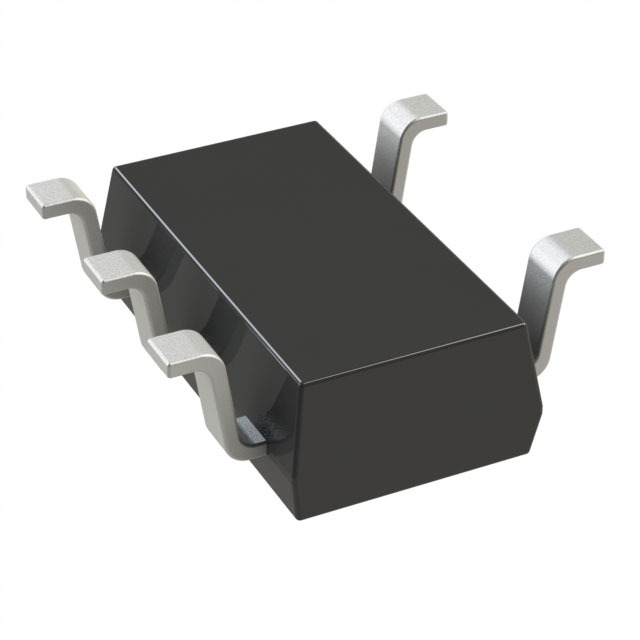
- Package: SOT-23-5
- Essence: Voltage level shifting between two logic levels
- Packaging/Quantity: Tape and Reel, 3000 units per reel
Specifications
- Supply Voltage Range: 1.65V to 5.5V
- Logic Input Voltage Range (VIL): 0V to 0.8V
- Logic Input Voltage Range (VIH): 2V to VCC + 0.3V
- Output Voltage Range (VO): 0V to VCC
- Maximum Output Current (IO): ±25mA
- Propagation Delay (tPD): 4.5ns (typical)
- Operating Temperature Range: -40°C to +85°C
Detailed Pin Configuration
The 74V1T05STR IC has a total of 5 pins in the SOT-23 package: 1. Pin 1: GND (Ground) 2. Pin 2: A (Input) 3. Pin 3: B (Output) 4. Pin 4: VCC (Power Supply) 5. Pin 5: NC (No Connection)
Functional Features
- The 74V1T05STR is designed to shift logic levels from one voltage domain to another.
- It provides non-inverting voltage translation with an open-drain output.
- The device operates bidirectionally, allowing voltage level shifting in both directions.
- It can be used to interface between systems operating at different voltage levels.
Advantages and Disadvantages
Advantages: - Wide supply voltage range allows compatibility with various systems. - Non-inverting logic level shifting simplifies interfacing between different voltage domains. - Open-drain output enables easy connection to other devices. - Small SOT-23 package offers space-saving and flexibility in PCB design.
Disadvantages: - Limited maximum output current may restrict usage in high-current applications. - Propagation delay of 4.5ns may introduce timing issues in certain scenarios. - Lack of internal pull-up resistors may require additional components for specific applications.
Working Principles
The 74V1T05STR utilizes a combination of MOSFETs to achieve voltage level shifting. When the input voltage (A) is within the specified logic low range, the output (B) is pulled to ground through an open-drain NMOS transistor. Conversely, when the input voltage is within the logic high range, the output is left floating, allowing external pull-up resistors to determine the output voltage level.
Detailed Application Field Plans
The 74V1T05STR finds application in various scenarios where logic level translation is required. Some potential use cases include: 1. Interfacing between microcontrollers operating at different voltage levels. 2. Level shifting between digital sensors and microcontrollers. 3. Communication between different logic families (e.g., TTL and CMOS). 4. Voltage translation in battery-powered devices with varying voltage requirements.
Detailed and Complete Alternative Models
- SN74LVC1T45DBVR - Single-Bit Dual-Supply Bus Transceiver
- NC7SZ125P5X - Single-Bit Non-Inverting Buffer/Line Driver
- TXS0101DCTR - Single-Bit Bidirectional Voltage-Level Translator
These alternative models offer similar functionality and can be considered as substitutes for the 74V1T05STR in various applications.
Word Count: 408
Lista 10 Vanliga frågor och svar relaterade till tillämpningen av 74V1T05STR i tekniska lösningar
Sure! Here are 10 common questions and answers related to the application of 74V1T05STR in technical solutions:
Q1: What is the 74V1T05STR? A1: The 74V1T05STR is a hex non-inverting buffer with open-drain outputs. It is commonly used in digital logic circuits.
Q2: What is the purpose of using the 74V1T05STR? A2: The 74V1T05STR is used to provide buffering and level shifting capabilities in digital circuits, ensuring proper signal transmission between different components.
Q3: What voltage levels can the 74V1T05STR handle? A3: The 74V1T05STR can handle voltage levels ranging from 2V to 5.5V, making it compatible with a wide range of digital systems.
Q4: How many inputs and outputs does the 74V1T05STR have? A4: The 74V1T05STR has six inputs and six open-drain outputs, making it suitable for applications requiring multiple signal lines.
Q5: Can the 74V1T05STR be used for bidirectional communication? A5: No, the 74V1T05STR is a unidirectional buffer and cannot be used for bidirectional communication. For bidirectional communication, a different type of buffer or transceiver should be used.
Q6: What is the maximum current that the 74V1T05STR can sink/source? A6: The 74V1T05STR can sink/source up to 24mA of current per output pin, allowing it to drive moderate loads.
Q7: Is the 74V1T05STR tolerant to overvoltage conditions? A7: No, the 74V1T05STR is not tolerant to overvoltage conditions. It is recommended to ensure that the input voltage does not exceed the specified limits to prevent damage.
Q8: Can the 74V1T05STR be used in high-speed applications? A8: Yes, the 74V1T05STR can be used in high-speed applications as it has a propagation delay of only a few nanoseconds, making it suitable for fast digital signals.
Q9: Are there any special considerations when using the 74V1T05STR in noisy environments? A9: Yes, in noisy environments, it is recommended to use proper decoupling capacitors and filtering techniques to minimize the impact of noise on the performance of the 74V1T05STR.
Q10: Can multiple 74V1T05STR chips be cascaded together? A10: Yes, multiple 74V1T05STR chips can be cascaded together to increase the number of buffered outputs or to drive more complex digital circuits.