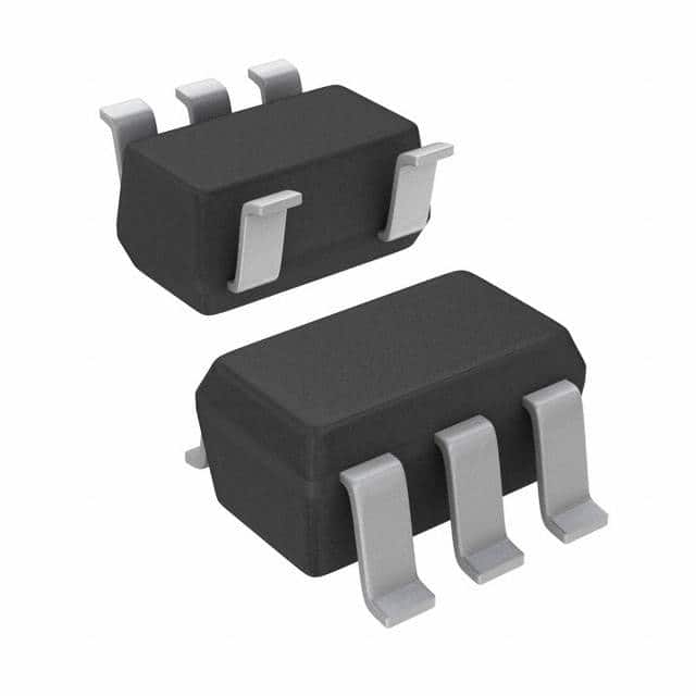
74AHC1G125DBVRG4
Basic Information Overview
- Category: Integrated Circuit (IC)
- Use: Logic Level Shifter
- Characteristics: Single Bus Buffer Gate with 3-State Output
- Package: SOT-23 (Thin, Small Outline Transistor)
- Essence: This IC is designed to provide level shifting capabilities for digital signals in various electronic circuits.
- Packaging/Quantity: Available in tape and reel packaging, with a quantity of 3000 units per reel.
Specifications
- Supply Voltage Range: 2 V to 5.5 V
- High-Level Input Voltage: 0.7 x VCC to VCC + 0.3 V
- Low-Level Input Voltage: -0.3 V to 0.3 V
- High-Level Output Voltage: VCC - 0.3 V
- Low-Level Output Voltage: 0.3 V
- Maximum Operating Frequency: 400 MHz
- Maximum Propagation Delay: 6 ns
Detailed Pin Configuration
The 74AHC1G125DBVRG4 IC has the following pin configuration:
____
   OE |1  5| VCC
  IN1 |2  4| Y
  GND |3  6| NC
       ----
Functional Features
- Single gate buffer with 3-state output
- Provides level shifting between different voltage domains
- Enables bidirectional communication between devices operating at different logic levels
- Supports high-speed data transmission up to 400 MHz
- Low power consumption
- Wide supply voltage range allows compatibility with various systems
Advantages
- Compact package size enables space-saving designs
- 3-state output allows multiple devices to share a common bus
- Wide supply voltage range provides flexibility in system integration
- High-speed operation facilitates efficient data transfer
- Low power consumption helps prolong battery life in portable devices
Disadvantages
- Limited number of input/output pins (single gate)
- Not suitable for applications requiring multiple gates or complex logic functions
- May require additional external components for specific applications
Working Principles
The 74AHC1G125DBVRG4 is a single bus buffer gate that operates as a level shifter. It takes digital signals from one voltage domain and shifts them to another voltage domain, allowing communication between devices operating at different logic levels. The IC uses a combination of transistors and resistors to achieve the desired voltage translation.
Detailed Application Field Plans
The 74AHC1G125DBVRG4 IC finds applications in various electronic systems, including: 1. Battery-powered devices: Enables level shifting between low-voltage microcontrollers and higher voltage peripherals. 2. Communication systems: Facilitates signal conversion between different logic families, such as TTL and CMOS. 3. Industrial automation: Allows interfacing between different voltage domains in control systems. 4. Automotive electronics: Provides level shifting capabilities for communication between sensors and microcontrollers. 5. Consumer electronics: Enables compatibility between devices with different logic voltage requirements, such as smartphones and accessories.
Detailed and Complete Alternative Models
Some alternative models that provide similar functionality to the 74AHC1G125DBVRG4 IC include: - SN74LVC1G125DBVR - MC74VHC1G125DTT1G - TC7SZ125FU
These alternatives offer comparable features and can be used as replacements depending on specific application requirements.
Word count: 498 words
Lista 10 Vanliga frågor och svar relaterade till tillämpningen av 74AHC1G125DBVRG4 i tekniska lösningar
Sure! Here are 10 common questions and answers related to the application of 74AHC1G125DBVRG4 in technical solutions:
Q1: What is the 74AHC1G125DBVRG4? A1: The 74AHC1G125DBVRG4 is a single bus buffer gate with 3-state output, designed for low-power applications.
Q2: What is the operating voltage range of the 74AHC1G125DBVRG4? A2: The operating voltage range is from 2.0V to 5.5V.
Q3: What is the maximum output current of the 74AHC1G125DBVRG4? A3: The maximum output current is 8mA.
Q4: Can the 74AHC1G125DBVRG4 be used as a level shifter? A4: Yes, the 74AHC1G125DBVRG4 can be used as a level shifter to convert signals between different voltage levels.
Q5: What is the propagation delay of the 74AHC1G125DBVRG4? A5: The propagation delay is typically 6 ns.
Q6: Can the 74AHC1G125DBVRG4 be used in high-speed applications? A6: Yes, the 74AHC1G125DBVRG4 can be used in high-speed applications due to its fast propagation delay.
Q7: Does the 74AHC1G125DBVRG4 have built-in ESD protection? A7: Yes, the 74AHC1G125DBVRG4 has built-in ESD protection to prevent damage from electrostatic discharge.
Q8: Can the 74AHC1G125DBVRG4 drive capacitive loads? A8: Yes, the 74AHC1G125DBVRG4 can drive capacitive loads up to 50pF.
Q9: Is the 74AHC1G125DBVRG4 compatible with other logic families? A9: Yes, the 74AHC1G125DBVRG4 is compatible with both CMOS and TTL logic families.
Q10: What is the package type of the 74AHC1G125DBVRG4? A10: The 74AHC1G125DBVRG4 is available in a SOT-23-5 package.
Please note that these answers are general and may vary depending on the specific datasheet and manufacturer's specifications.


