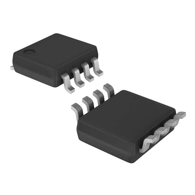
74AUC2G240DCURG4
Basic Information Overview
- Category: Integrated Circuit (IC)
- Use: Logic Gate
- Characteristics: Dual Inverting Buffer/Line Driver
- Package: SOT-353
- Essence: High-Speed CMOS Technology
- Packaging/Quantity: Tape and Reel, 3000 pieces per reel
Specifications
- Supply Voltage Range: 0.8V to 3.6V
- Input Voltage Range: -0.5V to VCC + 0.5V
- Output Voltage Range: 0V to VCC
- Maximum Operating Frequency: 1.5GHz
- Propagation Delay: 1.5ns (typical)
- Input Capacitance: 1.5pF (typical)
- Output Current: ±24mA (maximum)
Detailed Pin Configuration
The 74AUC2G240DCURG4 has a total of 6 pins: 1. GND (Ground) 2. A Input 3. Y Output 4. B Input 5. Y Output 6. VCC (Power Supply)
Functional Features
- Dual inverting buffer/line driver with high-speed operation.
- Compatible with various logic families due to its wide supply voltage range.
- Low power consumption and high noise immunity.
- Provides excellent signal integrity and reliability.
Advantages
- Wide supply voltage range allows for compatibility with different systems.
- High-speed operation enables efficient data transmission.
- Low power consumption contributes to energy efficiency.
- Excellent signal integrity ensures reliable performance.
Disadvantages
- Limited output current may restrict use in certain applications.
- Propagation delay may affect timing-sensitive operations.
- Input capacitance can impact circuit design in high-frequency applications.
Working Principles
The 74AUC2G240DCURG4 is based on high-speed CMOS technology. It functions as a dual inverting buffer/line driver, providing signal amplification and level shifting capabilities. The IC operates within a wide supply voltage range, allowing it to interface with various logic families. By utilizing complementary metal-oxide-semiconductor (CMOS) technology, the IC achieves low power consumption and high noise immunity.
Detailed Application Field Plans
The 74AUC2G240DCURG4 finds applications in various fields, including: 1. Communication systems 2. Data transmission networks 3. Industrial automation 4. Consumer electronics 5. Automotive electronics
Detailed and Complete Alternative Models
- SN74LVC2G240DCUR: Dual Inverting Buffer/Line Driver, SOT-353 package.
- MC74VHC2G240DCURG4: Dual Inverting Buffer/Line Driver, SOT-353 package.
- TC7SZU04FU(T5L,F): Dual Inverter, UDFN6 package.
- NC7SZU04P5X: Single Inverter, SC70-5 package.
- CD74HCT04M96: Hex Inverter, SOIC-14 package.
(Note: This list is not exhaustive and other alternative models may exist.)
This entry provides an overview of the 74AUC2G240DCURG4 integrated circuit, including its basic information, specifications, pin configuration, functional features, advantages, disadvantages, working principles, application field plans, and alternative models. With its high-speed operation, wide supply voltage range, and compatibility with various logic families, the 74AUC2G240DCURG4 is a versatile logic gate suitable for numerous applications in different industries.
Lista 10 Vanliga frågor och svar relaterade till tillämpningen av 74AUC2G240DCURG4 i tekniska lösningar
Sure! Here are 10 common questions and answers related to the application of 74AUC2G240DCURG4 in technical solutions:
Q: What is the 74AUC2G240DCURG4? A: The 74AUC2G240DCURG4 is a dual inverting buffer and line driver integrated circuit (IC) that operates at a low voltage and is commonly used in digital logic applications.
Q: What is the operating voltage range of the 74AUC2G240DCURG4? A: The 74AUC2G240DCURG4 operates within a voltage range of 0.8V to 3.6V, making it suitable for low-power and battery-operated devices.
Q: What is the maximum output current of the 74AUC2G240DCURG4? A: The 74AUC2G240DCURG4 can provide a maximum output current of 24mA, allowing it to drive various loads.
Q: Can the 74AUC2G240DCURG4 be used as a level shifter? A: Yes, the 74AUC2G240DCURG4 can be used as a level shifter to convert signals between different voltage levels, making it useful in interfacing different components or systems.
Q: Does the 74AUC2G240DCURG4 have built-in protection features? A: Yes, the 74AUC2G240DCURG4 has built-in protection against electrostatic discharge (ESD), which helps safeguard the IC from damage during handling or operation.
Q: What is the typical propagation delay of the 74AUC2G240DCURG4? A: The typical propagation delay of the 74AUC2G240DCURG4 is around 1.5 nanoseconds, making it suitable for high-speed digital applications.
Q: Can the 74AUC2G240DCURG4 be used in both CMOS and TTL logic systems? A: Yes, the 74AUC2G240DCURG4 is compatible with both CMOS and TTL logic levels, allowing it to interface with a wide range of devices.
Q: Is the 74AUC2G240DCURG4 available in different package options? A: Yes, the 74AUC2G240DCURG4 is available in various package options, such as SOT-23 and X2SON, providing flexibility for different PCB layouts and space constraints.
Q: Can the 74AUC2G240DCURG4 operate in harsh environments? A: The 74AUC2G240DCURG4 has a wide operating temperature range of -40°C to 125°C, allowing it to function reliably in a variety of environmental conditions.
Q: What are some common applications of the 74AUC2G240DCURG4? A: The 74AUC2G240DCURG4 is commonly used in applications such as data communication, signal buffering, level shifting, clock distribution, and general-purpose digital logic circuits.
Please note that the answers provided here are general and may vary depending on specific datasheet specifications and application requirements.


