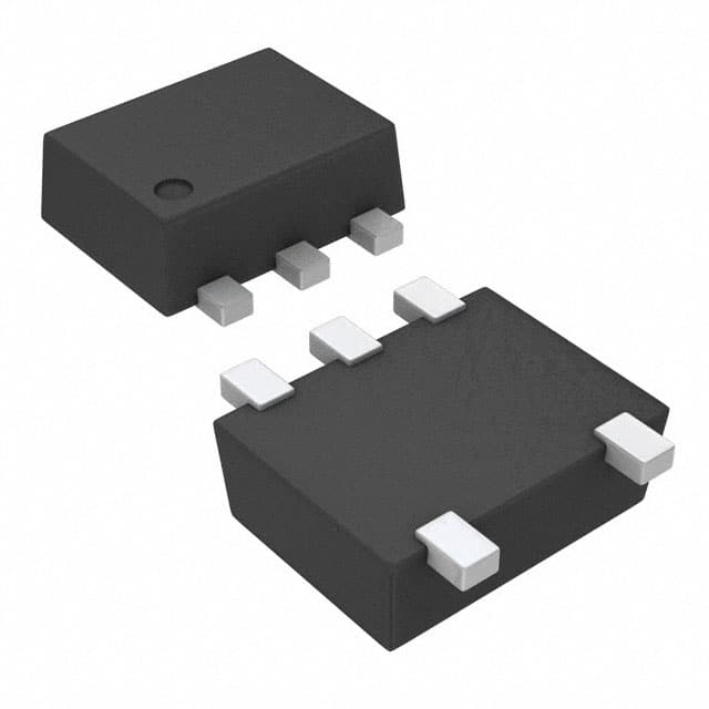
74LVC1GU04DRLRG4
Product Overview
Category
The 74LVC1GU04DRLRG4 belongs to the category of integrated circuits (ICs) and specifically falls under the logic gates subcategory.
Use
This product is commonly used in digital electronics for signal processing and logical operations. It serves as an inverter gate, which means it can convert a logic level from high to low or vice versa.
Characteristics
- Low voltage operation: The 74LVC1GU04DRLRG4 operates at a low voltage range, typically between 1.65V and 5.5V.
- High-speed performance: It offers fast switching times, making it suitable for applications requiring quick response times.
- Low power consumption: This IC is designed to consume minimal power, making it energy-efficient.
- Small form factor: The package size is compact, allowing for space-saving integration into electronic devices.
Package
The 74LVC1GU04DRLRG4 is available in a small outline package (SOT-553), which consists of three pins for input, output, and ground connections.
Essence
The essence of the 74LVC1GU04DRLRG4 lies in its ability to invert logic levels, enabling various logical operations in digital circuits.
Packaging/Quantity
This product is typically sold in reels containing a specific quantity, such as 3000 units per reel.
Specifications
- Supply Voltage Range: 1.65V to 5.5V
- Input Voltage Range: 0V to VCC
- Output Voltage Range: 0V to VCC
- Operating Temperature Range: -40°C to +125°C
- Propagation Delay: 3.8ns (typical)
- Maximum Quiescent Current: 10μA
Detailed Pin Configuration
The 74LVC1GU04DRLRG4 has the following pin configuration:
+-----------------+
   VCC |1              6| GND
   IN  |2              5| OUT
   GND |3              4|
        +-----------------+
Functional Features
- Logic level inversion: The 74LVC1GU04DRLRG4 can invert the logic level of an input signal, providing the complemented output.
- High-speed operation: It offers fast switching times, allowing for efficient signal processing in digital circuits.
- Wide voltage range: This IC can operate within a broad voltage range, making it compatible with various systems.
- Low power consumption: The 74LVC1GU04DRLRG4 is designed to minimize power consumption, enhancing energy efficiency.
Advantages and Disadvantages
Advantages
- Compact size enables integration into space-constrained designs.
- Low power consumption contributes to energy-efficient operation.
- Wide voltage range compatibility enhances versatility.
- Fast switching times allow for quick response in digital circuits.
Disadvantages
- Limited functionality as it only serves as an inverter gate.
- May not be suitable for applications requiring complex logical operations.
Working Principles
The 74LVC1GU04DRLRG4 operates based on the principles of complementary metal-oxide-semiconductor (CMOS) technology. It utilizes a combination of p-type and n-type MOSFETs to achieve logic level inversion. When the input voltage is high, the p-MOSFET turns off, while the n-MOSFET turns on, resulting in a low output voltage. Conversely, when the input voltage is low, the p-MOSFET turns on, and the n-MOSFET turns off, producing a high output voltage.
Detailed Application Field Plans
The 74LVC1GU04DRLRG4 finds applications in various digital systems, including but not limited to: - Microcontrollers and microprocessors - Communication devices - Consumer electronics - Industrial automation - Automotive electronics
Detailed and Complete Alternative Models
Some alternative models that can be considered as substitutes for the 74LVC1GU04DRLRG4 include: - SN74LVC1G04DBVR - MC74VHC1G04DTT1G - TC7SZU04FUTE85LF
These alternatives offer similar functionality and characteristics, providing options for different design requirements.
Word count: 536 words
Lista 10 Vanliga frågor och svar relaterade till tillämpningen av 74LVC1GU04DRLRG4 i tekniska lösningar
Sure! Here are 10 common questions and answers related to the application of 74LVC1GU04DRLRG4 in technical solutions:
Q1: What is the 74LVC1GU04DRLRG4? A1: The 74LVC1GU04DRLRG4 is a single unbuffered inverter gate IC (Integrated Circuit) that operates at a voltage range of 1.65V to 5.5V.
Q2: What is the purpose of the 74LVC1GU04DRLRG4? A2: The purpose of this IC is to invert the input signal, i.e., it provides the complement of the input signal at its output.
Q3: What are the key features of the 74LVC1GU04DRLRG4? A3: Some key features include low power consumption, wide operating voltage range, high-speed operation, and compatibility with both CMOS and TTL logic levels.
Q4: What are the typical applications of the 74LVC1GU04DRLRG4? A4: This IC can be used in various applications such as level shifting, signal inversion, clock generation, pulse shaping, and interfacing between different logic families.
Q5: What is the maximum operating frequency of the 74LVC1GU04DRLRG4? A5: The maximum operating frequency of this IC is typically around 500 MHz.
Q6: Can the 74LVC1GU04DRLRG4 drive capacitive loads? A6: Yes, it can drive small capacitive loads up to a certain limit. However, for larger capacitive loads, additional buffering may be required.
Q7: What is the input voltage threshold for the 74LVC1GU04DRLRG4? A7: The input voltage threshold for this IC is typically around 0.8V when the supply voltage is 3.3V.
Q8: Can the 74LVC1GU04DRLRG4 tolerate overvoltage conditions? A8: No, this IC is not designed to tolerate overvoltage conditions. It is recommended to stay within the specified voltage range to ensure proper operation and avoid damage.
Q9: Is the 74LVC1GU04DRLRG4 available in different package options? A9: Yes, this IC is available in various package options such as SOT-23, SC-70, and X2SON.
Q10: What are some alternatives to the 74LVC1GU04DRLRG4? A10: Some alternatives to this IC include the 74HC04, 74HCT04, and SN74LVC1G04. These ICs also provide single inverter functionality but may have different specifications and features.
Please note that the answers provided here are general and may vary depending on specific datasheet information and application requirements.


