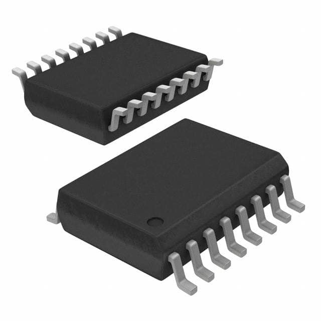
ADC12130CIWMX/NOPB
Product Overview
- Category: Analog-to-Digital Converter (ADC)
- Use: Converts analog signals into digital data for processing
- Characteristics: High-resolution, low-power consumption, small form factor
- Package: Ceramic 16-pin SOIC package
- Essence: Provides accurate and reliable conversion of analog signals to digital format
- Packaging/Quantity: Available in tape and reel packaging, quantity varies based on supplier
Specifications
- Resolution: 12 bits
- Sampling Rate: Up to 1 MSPS (Mega Samples Per Second)
- Input Voltage Range: 0V to VREF
- Power Supply: 2.7V to 5.5V
- Operating Temperature Range: -40°C to +85°C
- Interface: Serial Peripheral Interface (SPI)
Pin Configuration
The ADC12130CIWMX/NOPB has a total of 16 pins. The pin configuration is as follows:
- VDD: Power supply voltage
- AGND: Analog ground
- REF: Reference voltage input
- VIN: Analog input voltage
- VOUT: Digital output voltage
- CLK: Clock input for SPI interface
- CS: Chip select input for SPI interface
- DOUT: Serial data output
- DIN: Serial data input
- DGND: Digital ground
- NC: No connection
- NC: No connection
- NC: No connection
- NC: No connection
- NC: No connection
- NC: No connection
Functional Features
- High-resolution conversion with 12-bit accuracy
- Low power consumption for energy-efficient operation
- Small form factor allows for integration into compact designs
- Serial Peripheral Interface (SPI) for easy communication with microcontrollers
- Wide operating voltage range for flexibility in power supply options
Advantages and Disadvantages
Advantages: - High-resolution conversion ensures accurate digital representation of analog signals - Low power consumption prolongs battery life in portable devices - Small form factor enables integration into space-constrained applications - SPI interface simplifies communication with microcontrollers
Disadvantages: - Limited input voltage range may not be suitable for certain applications requiring higher voltage inputs - Higher cost compared to lower resolution ADCs - Requires external reference voltage for accurate conversion
Working Principles
The ADC12130CIWMX/NOPB operates by sampling the analog input voltage and converting it into a digital value using a 12-bit resolution. The analog signal is compared against a reference voltage, and the resulting digital value is output through the serial interface. The conversion process is controlled by the clock input and chip select signals provided through the SPI interface.
Detailed Application Field Plans
The ADC12130CIWMX/NOPB can be used in various applications that require accurate analog-to-digital conversion. Some potential application fields include:
- Industrial Automation: Monitoring and control systems that require precise measurement of analog signals.
- Medical Devices: Vital sign monitoring equipment, patient monitoring systems, and medical imaging devices.
- Test and Measurement Instruments: Oscilloscopes, data loggers, and signal analyzers that need high-resolution data acquisition.
- Communication Systems: Wireless base stations, satellite communication systems, and network analyzers.
- Automotive Electronics: Engine control units, sensor interfaces, and battery management systems.
Detailed and Complete Alternative Models
- ADC12132CIWMX/NOPB: Similar to ADC12130CIWMX/NOPB but with 12-bit resolution and higher sampling rate.
- ADC12128CIWMX/NOPB: Lower-cost alternative with 12-bit resolution and lower sampling rate.
- ADC12134CIWMX/NOPB: Higher-resolution option with 14-bit resolution and similar characteristics.
These alternative models provide options with varying resolutions, sampling rates, and cost considerations to suit different application requirements.
Word count: 529 words
Lista 10 Vanliga frågor och svar relaterade till tillämpningen av ADC12130CIWMX/NOPB i tekniska lösningar
Question: What is the maximum sampling rate of ADC12130CIWMX/NOPB?
Answer: The maximum sampling rate of ADC12130CIWMX/NOPB is 1 MSPS (mega samples per second).Question: What is the resolution of ADC12130CIWMX/NOPB?
Answer: ADC12130CIWMX/NOPB has a resolution of 12 bits.Question: What is the input voltage range of ADC12130CIWMX/NOPB?
Answer: The input voltage range of ADC12130CIWMX/NOPB is 0 to VREF.Question: Can ADC12130CIWMX/NOPB operate at low power?
Answer: Yes, ADC12130CIWMX/NOPB is designed for low power operation.Question: What is the supply voltage range for ADC12130CIWMX/NOPB?
Answer: The supply voltage range for ADC12130CIWMX/NOPB is 2.7V to 5.25V.Question: Does ADC12130CIWMX/NOPB have an internal reference voltage?
Answer: Yes, ADC12130CIWMX/NOPB has an internal 2.5V reference voltage.Question: Is ADC12130CIWMX/NOPB suitable for battery-powered applications?
Answer: Yes, ADC12130CIWMX/NOPB is suitable for battery-powered applications due to its low power consumption.Question: What is the typical power consumption of ADC12130CIWMX/NOPB?
Answer: The typical power consumption of ADC12130CIWMX/NOPB is 1.6 mW at 1 MSPS.Question: Can ADC12130CIWMX/NOPB be used in industrial temperature range applications?
Answer: Yes, ADC12130CIWMX/NOPB is specified for the industrial temperature range of -40°C to 85°C.Question: Does ADC12130CIWMX/NOPB support SPI interface?
Answer: Yes, ADC12130CIWMX/NOPB supports SPI interface for communication with microcontrollers or other devices.


