

ADS5421Y/R
Product Overview
Category: Analog-to-Digital Converter (ADC)
Use: The ADS5421Y/R is a high-speed, high-resolution ADC designed for various applications in the field of data acquisition and signal processing. It converts analog signals into digital format with exceptional accuracy and speed.
Characteristics: - High resolution: The ADS5421Y/R offers a resolution of up to 16 bits, ensuring precise conversion of analog signals. - High sampling rate: With a maximum sampling rate of 250 mega-samples per second (MSPS), it can capture fast-changing signals accurately. - Low power consumption: The device operates at low power levels, making it suitable for portable and battery-powered applications. - Wide input voltage range: It supports a wide input voltage range, allowing for versatile usage across different signal levels. - Integrated features: The ADC incorporates various integrated features such as programmable gain amplifiers, reference voltage generators, and digital interfaces.
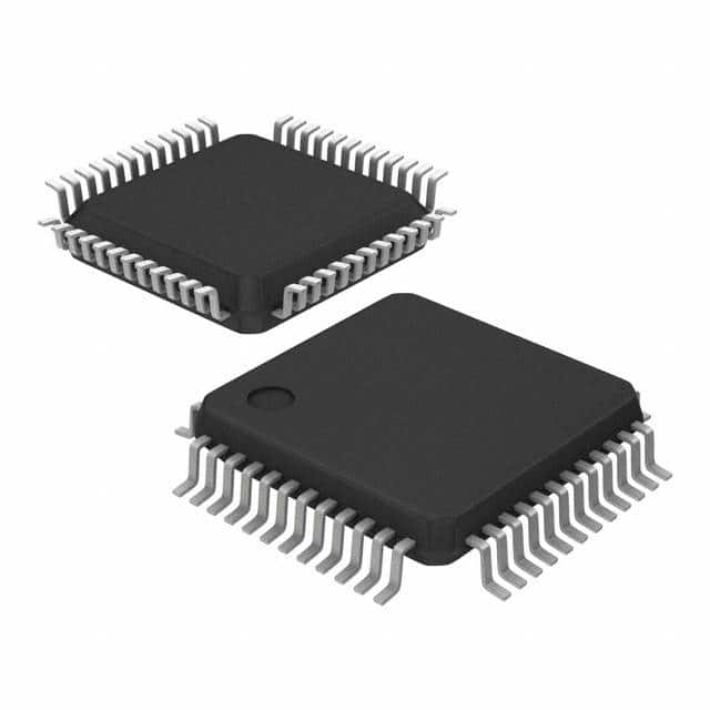
Package: The ADS5421Y/R is available in a compact and robust package, ensuring easy integration into electronic systems. It is offered in a small outline package (SOP) or quad flat no-lead (QFN) package.
Essence: The essence of the ADS5421Y/R lies in its ability to accurately convert analog signals into digital form, enabling further processing and analysis.
Packaging/Quantity: The ADC is typically sold in reels or trays, with quantities varying based on customer requirements.
Specifications
- Resolution: Up to 16 bits
- Sampling Rate: Up to 250 MSPS
- Input Voltage Range: ±5V
- Power Supply: +3.3V
- Operating Temperature Range: -40°C to +85°C
- Interface: Serial Peripheral Interface (SPI)
- Package Type: SOP/QFN
Pin Configuration
The ADS5421Y/R features a 32-pin package with the following pin configuration:
```
Pin Name Description
1 VREFP Positive Reference Voltage 2 VREFN Negative Reference Voltage 3 AGND Analog Ground 4 VIN+ Positive Analog Input 5 VIN- Negative Analog Input 6 VCM Common Mode Voltage 7 DVDD Digital Power Supply 8 DGND Digital Ground 9 CLK Clock Input 10 CS Chip Select 11 SDI Serial Data Input 12 SDO Serial Data Output 13 SCLK Serial Clock 14 PDWN Power Down 15 RESET Reset 16 D0 Digital Output Bit 0 17 D1 Digital Output Bit 1 18 D2 Digital Output Bit 2 19 D3 Digital Output Bit 3 20 D4 Digital Output Bit 4 21 D5 Digital Output Bit 5 22 D6 Digital Output Bit 6 23 D7 Digital Output Bit 7 24 D8 Digital Output Bit 8 25 D9 Digital Output Bit 9 26 D10 Digital Output Bit 10 27 D11 Digital Output Bit 11 28 D12 Digital Output Bit 12 29 D13 Digital Output Bit 13 30 D14 Digital Output Bit 14 31 D15 Digital Output Bit 15 32 DVDD Digital Power Supply ```
Functional Features
The ADS5421Y/R offers several functional features that enhance its performance and usability:
- Programmable Gain Amplifiers: The ADC includes programmable gain amplifiers to adjust the input signal level, allowing for optimal signal-to-noise ratio and dynamic range.
- Reference Voltage Generators: Integrated reference voltage generators ensure accurate and stable voltage references for precise conversion.
- Digital Interfaces: The ADC supports a serial peripheral interface (SPI) for easy communication with microcontrollers or digital signal processors.
- Power-Down Mode: The device features a power-down mode to conserve power when not in use.
- Reset Functionality: A reset pin allows for resetting the ADC to its default state.
Advantages and Disadvantages
Advantages: - High resolution and sampling rate enable accurate and detailed signal capture. - Low power consumption makes it suitable for portable and battery-powered applications. - Wide input voltage range allows for versatile usage across different signal levels. - Integrated features simplify system design and reduce external component count.
Disadvantages: - Limited number of digital output bits may restrict certain applications requiring higher bit resolutions. - Higher cost compared to lower-end ADCs with lower specifications.
Working Principles
The ADS5421Y/R operates based on the successive approximation register (SAR) architecture. It samples the
Lista 10 Vanliga frågor och svar relaterade till tillämpningen av ADS5421Y/R i tekniska lösningar
What is the operating voltage range of ADS5421Y/R?
- The operating voltage range of ADS5421Y/R is 2.7V to 5.5V.What is the maximum sampling rate of ADS5421Y/R?
- The maximum sampling rate of ADS5421Y/R is 65MSPS (mega samples per second).Can ADS5421Y/R be used in low-power applications?
- Yes, ADS5421Y/R can be used in low-power applications as it has a low power consumption of 95mW at 65MSPS.Does ADS5421Y/R support SPI interface?
- Yes, ADS5421Y/R supports SPI interface for communication with microcontrollers or other devices.What is the resolution of ADS5421Y/R?
- ADS5421Y/R has a resolution of 12 bits.Is ADS5421Y/R suitable for high-speed data acquisition systems?
- Yes, ADS5421Y/R is suitable for high-speed data acquisition systems due to its high sampling rate and resolution.Can ADS5421Y/R be used in industrial control and automation applications?
- Yes, ADS5421Y/R can be used in industrial control and automation applications due to its performance and reliability.What is the input voltage range of ADS5421Y/R?
- The input voltage range of ADS5421Y/R is 0V to VREF.Does ADS5421Y/R have built-in digital filters?
- Yes, ADS5421Y/R has built-in digital filters to improve signal quality and reduce noise.Is ADS5421Y/R RoHS compliant?
- Yes, ADS5421Y/R is RoHS compliant, making it suitable for use in environmentally sensitive applications.