

ADS5433IPJYRG3
Product Overview
- Category: Integrated Circuit (IC)
- Use: Analog-to-Digital Converter (ADC)
- Characteristics: High-speed, high-resolution ADC
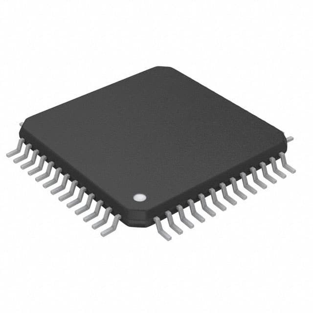
- Package: 32-pin LFCSP (Lead Frame Chip Scale Package)
- Essence: Converts analog signals into digital data
- Packaging/Quantity: Tape and Reel, 250 units per reel
Specifications
- Resolution: 14 bits
- Sampling Rate: 170 Mega Samples Per Second (MSPS)
- Input Voltage Range: ±2 V
- Power Supply: 3.3 V
- Operating Temperature Range: -40°C to +85°C
Pin Configuration
The ADS5433IPJYRG3 has a total of 32 pins. The pin configuration is as follows:
- REF-
- REF+
- AGND
- VIN-
- VIN+
- VCM
- VREFP
- VREFN
- CLKOUT
- CLKIN
- PDWN
- D[13]
- D[12]
- D[11]
- D[10]
- D[9]
- D[8]
- D[7]
- D[6]
- D[5]
- D[4]
- D[3]
- D[2]
- D[1]
- D[0]
- DVDD
- AVDD
- DGND
- VCMO
- VCOM
- VREF
- REFOUT
Functional Features
- High-speed conversion with a sampling rate of 170 MSPS
- High resolution of 14 bits for accurate signal representation
- Low power consumption for energy-efficient operation
- Wide input voltage range of ±2 V for versatile signal handling
- Differential inputs for improved noise rejection
- On-chip reference voltage generation for simplified design
Advantages and Disadvantages
Advantages: - High-speed and high-resolution conversion - Low power consumption - Wide input voltage range - On-chip reference voltage generation
Disadvantages: - Limited operating temperature range (-40°C to +85°C) - Requires external clock signal for operation
Working Principles
The ADS5433IPJYRG3 is an analog-to-digital converter that converts analog signals into digital data. It operates by sampling the analog input voltage at a high rate and quantizing it into discrete digital values. The converter uses a 14-bit resolution to accurately represent the input signal. The device also includes on-chip reference voltage generation, which simplifies the design process. The converted digital data can be further processed or stored for various applications.
Detailed Application Field Plans
The ADS5433IPJYRG3 is commonly used in applications that require high-speed and high-resolution analog-to-digital conversion. Some of the specific application fields include:
- Communications: Used in wireless communication systems for signal processing and modulation/demodulation.
- Test and Measurement: Used in oscilloscopes, spectrum analyzers, and other test equipment for accurate signal analysis.
- Medical Imaging: Used in medical imaging devices such as ultrasound machines and MRI scanners for capturing and processing analog signals.
- Industrial Automation: Used in industrial control systems for monitoring and controlling analog signals in real-time.
- Audio Processing: Used in professional audio equipment for high-fidelity sound recording and playback.
Detailed and Complete Alternative Models
- ADS5433IPJYG4: Similar to ADS5433IPJYRG3 with minor package variation (32-pin TQFP).
- ADS5433IPJYR: Similar to ADS5433IPJYRG3 with a different package (32-pin LQFP).
- ADS5433IPJYRGT: Similar to ADS5433IPJYRG3 with extended temperature range (-40°C to +125°C).
These alternative models offer similar functionality and performance but may have slight differences in package type or operating temperature range.
Word count: 433 words
Lista 10 Vanliga frågor och svar relaterade till tillämpningen av ADS5433IPJYRG3 i tekniska lösningar
Sure! Here are 10 common questions and answers related to the application of ADS5433IPJYRG3 in technical solutions:
Q: What is ADS5433IPJYRG3? A: ADS5433IPJYRG3 is a high-speed, low-power, 12-bit analog-to-digital converter (ADC) designed for various applications in the field of electronics.
Q: What is the maximum sampling rate of ADS5433IPJYRG3? A: The maximum sampling rate of ADS5433IPJYRG3 is 210 Mega Samples Per Second (MSPS).
Q: What is the power supply voltage range for ADS5433IPJYRG3? A: ADS5433IPJYRG3 operates with a power supply voltage range of 1.8V to 3.6V.
Q: Can ADS5433IPJYRG3 be used in battery-powered devices? A: Yes, ADS5433IPJYRG3 can be used in battery-powered devices due to its low-power consumption characteristics.
Q: What is the input voltage range of ADS5433IPJYRG3? A: The input voltage range of ADS5433IPJYRG3 is from -0.5V to VREF+0.5V.
Q: Does ADS5433IPJYRG3 support differential inputs? A: Yes, ADS5433IPJYRG3 supports differential inputs, which allows for better noise rejection and improved signal integrity.
Q: What is the resolution of ADS5433IPJYRG3? A: ADS5433IPJYRG3 has a resolution of 12 bits, providing accurate digital representation of analog signals.
Q: Can ADS5433IPJYRG3 be used in high-frequency applications? A: Yes, ADS5433IPJYRG3 is suitable for high-frequency applications due to its high sampling rate and low distortion characteristics.
Q: Does ADS5433IPJYRG3 have built-in digital signal processing features? A: No, ADS5433IPJYRG3 is a standalone ADC and does not have built-in digital signal processing features. It provides raw digital output data.
Q: What are some typical applications of ADS5433IPJYRG3? A: ADS5433IPJYRG3 can be used in various applications such as communications systems, medical imaging, test and measurement equipment, and radar systems.
Please note that these answers are general and may vary depending on the specific requirements and use cases.