

ADS7951QDBTRQ1
Product Overview
Category: Analog-to-Digital Converter (ADC)
Use: The ADS7951QDBTRQ1 is a high-performance, low-power, 12-bit ADC designed for automotive applications. It provides accurate conversion of analog signals into digital data.
Characteristics: - High resolution: 12-bit ADC - Low power consumption: Suitable for battery-powered applications - Automotive-grade: Designed to meet the stringent requirements of the automotive industry - Wide temperature range: Operates reliably in extreme temperature conditions - Small package size: Available in a compact QDBT package
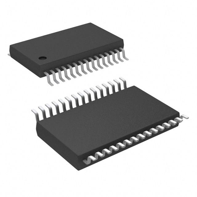
Package: The ADS7951QDBTRQ1 is available in a QDBT package, which stands for Quad Flat No-Lead (QFN) with exposed thermal pad.
Essence: The essence of the ADS7951QDBTRQ1 lies in its ability to accurately convert analog signals into digital data, making it suitable for various automotive applications.
Packaging/Quantity: The ADS7951QDBTRQ1 is typically sold in reels containing a quantity of 2500 units per reel.
Specifications
- Resolution: 12 bits
- Input voltage range: 0V to Vref
- Conversion rate: Up to 1 MSPS (Mega Samples Per Second)
- Supply voltage: 2.7V to 5.5V
- Operating temperature range: -40°C to +125°C
- Interface: SPI (Serial Peripheral Interface)
- Power consumption: 0.6 mW at 1 MSPS
Detailed Pin Configuration
The ADS7951QDBTRQ1 has a total of 16 pins. Here is the detailed pin configuration:
- VDD: Power supply voltage
- AGND: Analog ground
- REF: Reference voltage input
- VREF: Reference voltage output
- VIN: Analog input voltage
- D0-D11: Digital output data
- CS: Chip select input
- SCLK: Serial clock input
- SDI: Serial data input
- SDO: Serial data output
- DGND: Digital ground
Functional Features
- High-resolution conversion: The 12-bit ADC provides accurate and precise digital conversion of analog signals.
- Low power consumption: The ADS7951QDBTRQ1 is designed to minimize power consumption, making it suitable for battery-powered applications.
- Automotive-grade reliability: It meets the stringent requirements of the automotive industry, ensuring reliable performance in automotive applications.
- Wide temperature range: The ADC operates reliably in extreme temperature conditions, making it suitable for automotive environments.
Advantages and Disadvantages
Advantages: - High resolution for accurate conversion - Low power consumption - Automotive-grade reliability - Wide temperature range operation
Disadvantages: - Limited number of channels (single-channel ADC) - Requires an external reference voltage
Working Principles
The ADS7951QDBTRQ1 works by sampling the analog input voltage and converting it into a digital representation using its internal ADC circuitry. The analog input voltage is compared to a reference voltage, and the resulting digital value is outputted through the serial interface.
Detailed Application Field Plans
The ADS7951QDBTRQ1 is commonly used in various automotive applications, including: - Battery management systems - Engine control units - Powertrain systems - Sensor interfaces - Industrial automation
Detailed and Complete Alternative Models
Here are some alternative models that offer similar functionality to the ADS7951QDBTRQ1:
- ADS7950: 12-bit ADC with similar specifications and package options.
- ADS7949: 10-bit ADC with lower resolution but similar features.
- ADS7948: 8-bit ADC with lower resolution and lower power consumption.
These alternative models can be considered based on specific application requirements and cost considerations.
Word count: 529 words
Lista 10 Vanliga frågor och svar relaterade till tillämpningen av ADS7951QDBTRQ1 i tekniska lösningar
Sure! Here are 10 common questions and answers related to the application of ADS7951QDBTRQ1 in technical solutions:
1. What is the ADS7951QDBTRQ1? - The ADS7951QDBTRQ1 is a 12-bit, 8-channel analog-to-digital converter (ADC) with an integrated multiplexer.
2. What is the supply voltage range for the ADS7951QDBTRQ1? - The supply voltage range for the ADS7951QDBTRQ1 is from 2.7V to 5.5V.
3. How many channels does the ADS7951QDBTRQ1 have? - The ADS7951QDBTRQ1 has 8 input channels that can be individually selected using the built-in multiplexer.
4. What is the conversion rate of the ADS7951QDBTRQ1? - The ADS7951QDBTRQ1 has a maximum conversion rate of 1 MSPS (Mega Samples Per Second).
5. Does the ADS7951QDBTRQ1 support differential inputs? - Yes, the ADS7951QDBTRQ1 supports both single-ended and differential inputs.
6. What is the resolution of the ADS7951QDBTRQ1? - The ADS7951QDBTRQ1 has a resolution of 12 bits, providing 4096 possible output values.
7. Can the ADS7951QDBTRQ1 operate in a low-power mode? - Yes, the ADS7951QDBTRQ1 has a low-power mode that reduces the power consumption when not actively converting.
8. What is the interface used to communicate with the ADS7951QDBTRQ1? - The ADS7951QDBTRQ1 uses a serial interface called SPI (Serial Peripheral Interface) for communication with the microcontroller.
9. Does the ADS7951QDBTRQ1 have built-in reference voltage? - No, the ADS7951QDBTRQ1 requires an external reference voltage to be provided for accurate conversions.
10. Can the ADS7951QDBTRQ1 be used in automotive applications? - Yes, the ADS7951QDBTRQ1 is specifically designed for automotive applications and meets the AEC-Q100 qualification standards.
Please note that these answers are general and may vary depending on the specific application and requirements.