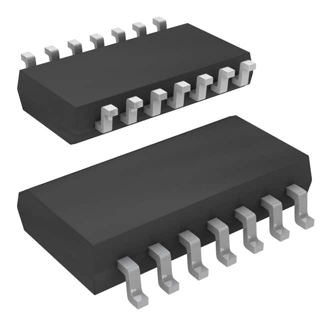
CD4002BNSR
Product Overview
Category
CD4002BNSR belongs to the category of integrated circuits (ICs).
Use
This IC is commonly used in digital logic applications.
Characteristics
- CD4002BNSR is a dual 4-input NOR gate.
- It operates at a supply voltage range of 3V to 18V.
- The IC has a wide operating temperature range of -55°C to +125°C.
Package
CD4002BNSR is available in a small outline package (SOIC) with 14 pins.
Essence
The essence of CD4002BNSR lies in its ability to perform logical operations using NOR gates, which are essential building blocks in digital circuit design.
Packaging/Quantity
CD4002BNSR is typically packaged in reels or tubes, with a quantity of 2500 units per reel/tube.
Specifications
- Supply Voltage Range: 3V to 18V
- Operating Temperature Range: -55°C to +125°C
- Logic Family: CMOS
- Number of Inputs: 4 per gate
- Number of Gates: 2
- Output Current: ±8mA
- Propagation Delay: 60ns (typical)
Detailed Pin Configuration
The pin configuration of CD4002BNSR is as follows:
``` __ __ A1| __/ |VDD A2| |Y1 B1| |Y2 B2| |GND C1| |D1 C2| |D2 D1| |C2 D2| |C1 Y1| |B2 Y2| |B1 GND |A2 VDD |A1
```
Functional Features
- CD4002BNSR provides two independent 4-input NOR gates in a single IC package.
- It offers high noise immunity and low power consumption due to its CMOS technology.
- The IC has a wide supply voltage range, making it suitable for various applications.
- CD4002BNSR exhibits excellent speed performance with a low propagation delay.
Advantages and Disadvantages
Advantages
- Compact size and integration of multiple NOR gates in one package.
- Wide operating temperature range allows for versatile usage.
- Low power consumption makes it energy-efficient.
- High noise immunity ensures reliable operation in noisy environments.
Disadvantages
- Limited number of inputs per gate (4 inputs).
- Propagation delay may affect timing-sensitive applications.
Working Principles
CD4002BNSR operates based on the principles of NOR gate logic. Each gate within the IC performs logical operations on its respective inputs and produces an output based on the NOR truth table.
Detailed Application Field Plans
CD4002BNSR finds applications in various digital logic circuits, including but not limited to: - Arithmetic circuits - Memory systems - Data processing units - Control systems - Communication devices
Detailed and Complete Alternative Models
Some alternative models that can be considered as alternatives to CD4002BNSR are: - CD4001BNSR: Quad 2-input NOR gate - CD4007UBNSR: Dual complementary pair plus inverter - CD4011BNSR: Quad 2-input NAND gate - CD4015BNSR: Dual 4-stage static shift register
These alternative models offer similar functionality and can be used interchangeably depending on specific design requirements.
Word count: 431 words
Lista 10 Vanliga frågor och svar relaterade till tillämpningen av CD4002BNSR i tekniska lösningar
Sure! Here are 10 common questions and answers related to the application of CD4002BNSR:
Q: What is CD4002BNSR? A: CD4002BNSR is a CMOS dual 4-input NOR gate integrated circuit commonly used in digital logic applications.
Q: What is the operating voltage range for CD4002BNSR? A: The operating voltage range for CD4002BNSR is typically between 3V and 18V.
Q: Can CD4002BNSR be used as an AND gate? A: No, CD4002BNSR is specifically designed as a NOR gate and cannot be used as an AND gate.
Q: How many inputs does CD4002BNSR have? A: CD4002BNSR has four inputs, allowing you to perform logical operations on up to four binary inputs.
Q: What is the maximum output current of CD4002BNSR? A: The maximum output current of CD4002BNSR is typically around 6mA.
Q: Can CD4002BNSR be used in high-speed applications? A: Yes, CD4002BNSR can be used in high-speed applications as it has a propagation delay of around 60ns.
Q: Is CD4002BNSR compatible with TTL logic levels? A: Yes, CD4002BNSR is compatible with TTL logic levels, making it suitable for interfacing with other TTL devices.
Q: Can CD4002BNSR be used in battery-powered applications? A: Yes, CD4002BNSR can be used in battery-powered applications as it operates at low power and has a wide voltage range.
Q: What is the package type of CD4002BNSR? A: CD4002BNSR is available in a 14-pin DIP (Dual In-line Package) or SOIC (Small Outline Integrated Circuit) package.
Q: Are there any recommended decoupling capacitors for CD4002BNSR? A: It is generally recommended to use a 0.1μF ceramic capacitor placed close to the power supply pins of CD4002BNSR to ensure stable operation.
Please note that these answers are general and may vary depending on specific datasheet specifications and application requirements.


