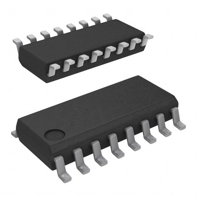
CD40175BM96
Product Overview
- Category: Integrated Circuit
- Use: Digital Logic Flip-Flop
- Characteristics: High-speed, low-power consumption
- Package: SOIC-16
- Essence: Flip-flop with quad D-type transparent latch
- Packaging/Quantity: Tape and Reel, 2500 units per reel
Specifications
- Supply Voltage: 3V to 18V
- Logic Family: CMOS
- Number of Flip-Flops: 4
- Latch Type: Transparent
- Data Input Format: Standard TTL or CMOS
- Output Type: Complementary
- Propagation Delay: 10 ns (typical)
- Operating Temperature Range: -40°C to +85°C
Detailed Pin Configuration
The CD40175BM96 has a total of 16 pins. The pin configuration is as follows:
- CLR (Clear) - Clear input
- D (Data) - Data input
- CP (Clock Pulse) - Clock pulse input
- Q (Output) - Output
- GND (Ground) - Ground reference
- Q̅ (Complementary Output) - Complementary output
- D (Data) - Data input
- CP (Clock Pulse) - Clock pulse input
- Q (Output) - Output
- GND (Ground) - Ground reference
- Q̅ (Complementary Output) - Complementary output
- D (Data) - Data input
- CP (Clock Pulse) - Clock pulse input
- Q (Output) - Output
- GND (Ground) - Ground reference
- VDD (Supply Voltage) - Positive supply voltage
Functional Features
- Quad D-type transparent latch with complementary outputs
- Non-inverting data path for each latch
- Asynchronous clear input to reset all latches
- High-speed operation with low power consumption
- Wide supply voltage range allows compatibility with various systems
Advantages and Disadvantages
Advantages
- High-speed operation enables efficient data processing
- Low power consumption reduces energy usage
- Wide supply voltage range provides flexibility in system integration
- Compact SOIC-16 package saves board space
Disadvantages
- Limited number of flip-flops (4) may not be sufficient for complex applications
- Lack of built-in protection features against electrical faults
Working Principles
The CD40175BM96 is a quad D-type transparent latch that stores and outputs digital data. It operates based on the clock pulse input, which transfers the data from the input to the output when the clock signal transitions. The latch can be cleared asynchronously using the clear input, resetting all the stored data.
Detailed Application Field Plans
The CD40175BM96 is commonly used in various digital systems and applications, including:
- Data storage and transfer in microcontrollers and microprocessors
- Register and buffer circuits in communication systems
- State machine implementation in digital logic designs
- Control and timing circuits in industrial automation
- Memory address decoding in memory subsystems
Detailed and Complete Alternative Models
- CD40174BM96: Hex D-type flip-flop with clear
- CD4013BM96: Dual D-type flip-flop with set and reset
- CD4027BM96: Dual J-K flip-flop with set and reset
- CD4042BM96: Quad D-type flip-flop with set and reset
These alternative models offer similar functionality and can be considered as substitutes for the CD40175BM96 in different applications.
Word count: 420 words
Lista 10 Vanliga frågor och svar relaterade till tillämpningen av CD40175BM96 i tekniska lösningar
Sure! Here are 10 common questions and answers related to the application of CD40175BM96 in technical solutions:
Q: What is CD40175BM96? A: CD40175BM96 is a quad D-type flip-flop integrated circuit (IC) that can store and manipulate digital data.
Q: What are the typical applications of CD40175BM96? A: CD40175BM96 is commonly used in digital systems, such as counters, registers, shift registers, and memory units.
Q: What is the operating voltage range for CD40175BM96? A: The operating voltage range for CD40175BM96 is typically between 3V and 18V.
Q: How many flip-flops are there in CD40175BM96? A: CD40175BM96 contains four independent D-type flip-flops.
Q: What is the maximum clock frequency supported by CD40175BM96? A: CD40175BM96 can operate at clock frequencies up to 25 MHz.
Q: Can CD40175BM96 be cascaded to create larger storage units? A: Yes, multiple CD40175BM96 ICs can be cascaded together to create larger storage units or registers.
Q: Does CD40175BM96 have any built-in asynchronous clear functionality? A: No, CD40175BM96 does not have a built-in asynchronous clear function. External logic may be required for clearing the flip-flops.
Q: What is the power supply current consumption of CD40175BM96? A: The power supply current consumption of CD40175BM96 varies depending on the operating conditions but typically ranges from a few microamps to a few milliamps.
Q: Can CD40175BM96 operate in both rising and falling edge-triggered modes? A: Yes, CD40175BM96 can be configured to operate in either rising or falling edge-triggered modes based on the clock input.
Q: Is CD40175BM96 available in different package types? A: Yes, CD40175BM96 is available in various package types, including SOIC (Small Outline Integrated Circuit) and TSSOP (Thin Shrink Small Outline Package).
Please note that the answers provided here are general and may vary depending on the specific datasheet and manufacturer's specifications for CD40175BM96.


