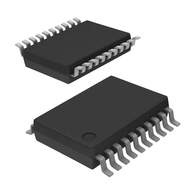
CD74ACT273SM96G4
Product Overview
- Category: Integrated Circuit
- Use: Flip-Flop
- Characteristics: High-speed, low-power consumption
- Package: Surface Mount
- Essence: Sequential Logic Device
- Packaging/Quantity: Tape and Reel, 2500 units per reel
Specifications
- Logic Family: ACT
- Number of Flip-Flops: 8
- Input Voltage: 2V - 6V
- Operating Temperature Range: -40°C to +85°C
- Propagation Delay: 5.5 ns (typical)
- Output Drive Capability: ±24 mA
Detailed Pin Configuration
The CD74ACT273SM96G4 has a total of 20 pins. The pin configuration is as follows:
- CLR (Clear)
- D0 (Data Input 0)
- D1 (Data Input 1)
- D2 (Data Input 2)
- D3 (Data Input 3)
- D4 (Data Input 4)
- D5 (Data Input 5)
- D6 (Data Input 6)
- D7 (Data Input 7)
- GND (Ground)
- Q7 (Output 7)
- Q6 (Output 6)
- Q5 (Output 5)
- Q4 (Output 4)
- Q3 (Output 3)
- Q2 (Output 2)
- Q1 (Output 1)
- Q0 (Output 0)
- CP (Clock Pulse)
- VCC (Power Supply)
Functional Features
- Eight edge-triggered D-type flip-flops with asynchronous clear functionality
- High-speed operation suitable for various applications
- Low power consumption for energy-efficient designs
- Wide operating voltage range for flexibility
Advantages and Disadvantages
Advantages
- High-speed operation allows for quick data processing
- Low power consumption helps in reducing energy costs
- Versatile design suitable for a wide range of applications
- Asynchronous clear functionality provides flexibility in resetting the flip-flops
Disadvantages
- Limited output drive capability may restrict use in certain high-current applications
- Propagation delay may affect timing-sensitive operations
Working Principles
The CD74ACT273SM96G4 is a sequential logic device that consists of eight D-type flip-flops. It operates on the rising edge of the clock pulse (CP) input, capturing the data present at the D0-D7 inputs and storing it in the corresponding flip-flop. The asynchronous clear (CLR) input allows for the simultaneous reset of all flip-flops to a known state.
Detailed Application Field Plans
The CD74ACT273SM96G4 can be used in various applications, including:
- Microprocessors and microcontrollers
- Data storage systems
- Communication equipment
- Industrial automation
- Automotive electronics
Detailed and Complete Alternative Models
Some alternative models that offer similar functionality to the CD74ACT273SM96G4 include:
- SN74ACT273: Similar specifications and pin configuration, available in different package options.
- MC74ACT273: Equivalent functionality with slight variations in electrical characteristics.
- 74HC273: Compatible with CMOS logic levels, suitable for mixed-voltage systems.
These alternative models provide options for designers based on specific requirements and availability.
Word count: 343 words
Lista 10 Vanliga frågor och svar relaterade till tillämpningen av CD74ACT273SM96G4 i tekniska lösningar
Sure! Here are 10 common questions and answers related to the application of CD74ACT273SM96G4 in technical solutions:
Q: What is CD74ACT273SM96G4? A: CD74ACT273SM96G4 is a type of octal D-type flip-flop integrated circuit (IC) that can store and manipulate digital data.
Q: What is the purpose of CD74ACT273SM96G4 in technical solutions? A: CD74ACT273SM96G4 is commonly used for data storage, synchronization, and control purposes in various digital systems and applications.
Q: How many flip-flops are there in CD74ACT273SM96G4? A: CD74ACT273SM96G4 consists of eight individual D-type flip-flops, making it an octal (8-bit) device.
Q: What is the operating voltage range for CD74ACT273SM96G4? A: CD74ACT273SM96G4 typically operates within a voltage range of 2V to 6V.
Q: What is the maximum clock frequency supported by CD74ACT273SM96G4? A: CD74ACT273SM96G4 can handle clock frequencies up to 100 MHz, depending on the specific datasheet specifications.
Q: Can CD74ACT273SM96G4 be used in both synchronous and asynchronous applications? A: Yes, CD74ACT273SM96G4 supports both synchronous and asynchronous operation modes, providing flexibility in different applications.
Q: What is the output drive capability of CD74ACT273SM96G4? A: CD74ACT273SM96G4 has a typical output drive capability of ±24 mA, allowing it to drive standard TTL or CMOS logic levels.
Q: Does CD74ACT273SM96G4 have any built-in protection features? A: Yes, CD74ACT273SM96G4 includes built-in ESD (electrostatic discharge) protection on all inputs and outputs, enhancing its reliability.
Q: Can CD74ACT273SM96G4 be cascaded with other flip-flops? A: Yes, CD74ACT273SM96G4 can be easily cascaded with other flip-flops to create larger storage registers or shift registers.
Q: What are some common applications of CD74ACT273SM96G4? A: CD74ACT273SM96G4 is commonly used in microprocessors, memory systems, data communication devices, control systems, and various digital circuits where data storage and manipulation are required.
Please note that the specific details and characteristics of CD74ACT273SM96G4 may vary based on the manufacturer's datasheet and application requirements.


